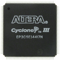
EP3C5E144I7N Altera, EP3C5E144I7N Datasheet - Page 71

EP3C5E144I7N
Manufacturer Part Number
EP3C5E144I7N
Description
IC CYCLONE III FPGA 5K 144 EQFP
Manufacturer
Altera
Series
Cyclone® IIIr
Datasheets
1.EP3C5F256C8N.pdf
(5 pages)
2.EP3C5F256C8N.pdf
(34 pages)
3.EP3C5F256C8N.pdf
(66 pages)
4.EP3C5F256C8N.pdf
(14 pages)
5.EP3C5F256C8N.pdf
(76 pages)
6.EP3C5E144I7N.pdf
(274 pages)
Specifications of EP3C5E144I7N
Number Of Logic Elements/cells
5136
Number Of Labs/clbs
321
Total Ram Bits
423936
Number Of I /o
94
Voltage - Supply
1.15 V ~ 1.25 V
Mounting Type
Surface Mount
Operating Temperature
-40°C ~ 100°C
Package / Case
144-EQFP
Family Name
Cyclone III
Number Of Logic Blocks/elements
5136
# I/os (max)
94
Frequency (max)
437.5MHz
Process Technology
65nm
Operating Supply Voltage (typ)
1.2V
Logic Cells
5136
Ram Bits
423936
Operating Supply Voltage (min)
1.15V
Operating Supply Voltage (max)
1.25V
Operating Temp Range
-40C to 100C
Operating Temperature Classification
Industrial
Mounting
Surface Mount
Pin Count
144
Package Type
EQFP
For Use With
544-2601 - KIT DEV CYCLONE III LS EP3CLS200544-2411 - KIT DEV NIOS II CYCLONE III ED.
Lead Free Status / RoHS Status
Lead free / RoHS Compliant
Number Of Gates
-
Lead Free Status / Rohs Status
Compliant
Other names
544-2557
Available stocks
Company
Part Number
Manufacturer
Quantity
Price
Company:
Part Number:
EP3C5E144I7N
Manufacturer:
Altera
Quantity:
135
Company:
Part Number:
EP3C5E144I7N
Manufacturer:
ALTERA32
Quantity:
345
Part Number:
EP3C5E144I7N
Manufacturer:
ALTERA/阿尔特拉
Quantity:
20 000
Chapter 5: Clock Networks and PLLs in the Cyclone III Device Family
Clock Networks
GCLK Network Power Down
© December 2009
f
Altera Corporation
The inputs to the five clock control blocks on each side must be chosen from among
the following clock sources:
■
■
■
■
From the clock sources listed above, only two clock input pins, two PLL clock
outputs, one DPCLK or CDPCLK pin, and one source from internal logic can drive into
any given clock control block, as shown in
Out of these five inputs to any clock control block, the two clock input pins and two
PLL outputs are dynamically selected to feed a GCLK. The clock control block
supports static selection of the signal from internal logic.
Figure 5–3
the Cyclone III device family periphery.
Figure 5–3. Clock Control Blocks on Each Side of the Cyclone III Device Family
Note to
(1) The left and right sides of the device have two DPCLK pins; the top and bottom of the device have four DPCLK pins.
You can disable the Cyclone III device family GCLK (power down) by using both
static and dynamic approaches. In the static approach, configuration bits are set in the
configuration file generated by the Quartus II software, which automatically disables
unused GCLKs. The dynamic clock enable or disable feature allows internal logic to
control clock enable or disable of the GCLKs in the Cyclone III device family.
When a clock network is disabled, all the logic fed by the clock network is in an
off-state, thereby reducing the overall power consumption of the device. This function
is independent of the PLL and is applied directly on the clock network, as shown in
Figure 5–1 on page
You can set the input clock sources and the clkena signals for the GCLK
multiplexers through the Quartus II software using the ALTCLKCTRL megafunction.
For more information, refer to the
Four clock input pins
Five PLL counter outputs
Two DPCLK pins and two CDPCLK pins from both the left and right sides, and four
DPCLK pins and two CDPCLK pins from both the top and bottom
Five signals from internal logic
Figure
shows a simplified version of the five clock control blocks on each side of
5–3:
5–5.
Clock Input Pins
Internal Logic
PLL Outputs
CDPCLK
DPCLK
ALTCLKCTRL Megafunction User
2 or 4
4
5
2
5
Blocks on Each Side
Five Clock Control
of the Device
Figure 5–1 on page
Control
Clock
Block
5
Cyclone III Device Handbook, Volume 1
GCLK
5–5.
Guide.
(Note 1)
5–7


