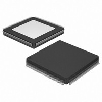
XC3S400-4PQ208C Xilinx Inc, XC3S400-4PQ208C Datasheet - Page 104

XC3S400-4PQ208C
Manufacturer Part Number
XC3S400-4PQ208C
Description
IC SPARTAN-3 FPGA 400K 208PQFP
Manufacturer
Xilinx Inc
Series
Spartan™-3r
Datasheet
1.XC3S50-4VQG100C.pdf
(217 pages)
Specifications of XC3S400-4PQ208C
Number Of Logic Elements/cells
8064
Number Of Labs/clbs
896
Total Ram Bits
294912
Number Of I /o
141
Number Of Gates
400000
Voltage - Supply
1.14 V ~ 1.26 V
Mounting Type
Surface Mount
Operating Temperature
0°C ~ 85°C
Package / Case
208-BFQFP
Other names
Q2844431
XC3S4004PQ208C
XC3S4004PQ208C
XC3S4004PQ208C
XC3S4004PQ208C
Available stocks
Company
Part Number
Manufacturer
Quantity
Price
Company:
Part Number:
XC3S400-4PQ208C
Manufacturer:
XILINX
Quantity:
392
Company:
Part Number:
XC3S400-4PQ208C
Manufacturer:
XILINX
Quantity:
5
Spartan-3 FPGA Family: Pinout Descriptions
Table 69: Spartan-3 FPGA Pin Definitions (Continued)
Detailed, Functional Pin Descriptions
I/O Type: Unrestricted, General-purpose I/O
Pins
After configuration, I/O-type pins are inputs, outputs, bidi-
rectional I/O, three-state outputs, open-drain outputs, or
open-source outputs, as defined in the application
Pins labeled "IO" support all SelectIO™ interface signal
standards except differential standards. A given device at
most only has a few of these pins.
A majority of the general-purpose I/O pins are labeled in the
format “IO_Lxxy_#”. These pins support all SelectIO signal
standards, including the differential standards such as
LVDS, ULVDS, BLVDS, RSDS, or LDT.
For additional information, see
Differential Pair Labeling
A pin supports differential standards if the pin is labeled in
the format “Lxxy_#”. The pin name suffix has the following
significance.
a differential input to and a differential output from Bank 2.
•
104
Notes:
1.
2.
VCCAUX: Auxiliary voltage supply pins
VCCAUX
VCCINT: Internal core voltage supply pins
VCCINT
GND: Ground supply pins
GND
N.C.: Unconnected package pins
N.C.
‘L’ indicates differential capability.
All unused inputs and bidirectional pins must be tied either High or Low. For unused enable inputs, apply the level that disables the
associated function. One common approach is to activate internal pull-up or pull-down resistors. An alternative approach is to
externally connect the pin to either VCCO or GND.
All outputs are of the totem-pole type — i.e., they can drive High as well as Low logic levels — except for the cases where “Open
Drain” is indicated. The latter can only drive a Low logic level and require a pull-up resistor to produce a High logic level.
Pin Name
Figure 38
provides a specific example showing
Supply
Supply
Supply
IOBs, page 12
Direction
www.xilinx.com
Power Supply for Auxiliary Circuits:
+2.5V power pins for auxiliary circuits, including the Digital Clock
Managers (DCMs), the dedicated configuration pins (CONFIG),
and the dedicated JTAG pins. All VCCAUX pins must be
connected.
Power Supply for Internal Core Logic:
+1.2V power pins for the internal logic. All pins must be connected.
Ground:
Ground pins, which are connected to the power supply’s return
path. All pins must be connected.
Unconnected Package Pin:
These package pins are unconnected.
•
•
•
If unused, these pins are in a high impedance state. The Bit-
stream generator option UnusedPin enables a pull-up or
pull-down resistor on all unused I/O pins.
Behavior from Power-On through End of Configu-
ration
During the configuration process, all pins that are not
actively involved in the configuration process are in a
high-impedance state. The CONFIG- and JTAG-type pins
have an internal pull-up resistor to VCCAUX during configu-
ration. For all other I/O pins, the HSWAP_EN input deter-
mines whether or not pull-up resistors are activated during
configuration. HSWAP_EN = 0 enables the pull-up resis-
tors. HSWAP_EN = 1 disables the pull-up resistors allowing
the pins to float, which is the desired state for hot-swap
applications.
"xx" is a two-digit integer, unique for each bank, that
identifies a differential pin-pair.
‘y’ is replaced by ‘P’ for the true signal or ‘N’ for the
inverted. These two pins form one differential pin-pair.
‘#’ is an integer, 0 through 7, indicating the associated
I/O bank.
Description
DS099-4 (v2.5) December 4, 2009
Product Specification
R


