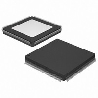
XC3S400-4PQ208C Xilinx Inc, XC3S400-4PQ208C Datasheet - Page 105

XC3S400-4PQ208C
Manufacturer Part Number
XC3S400-4PQ208C
Description
IC SPARTAN-3 FPGA 400K 208PQFP
Manufacturer
Xilinx Inc
Series
Spartan™-3r
Datasheet
1.XC3S50-4VQG100C.pdf
(217 pages)
Specifications of XC3S400-4PQ208C
Number Of Logic Elements/cells
8064
Number Of Labs/clbs
896
Total Ram Bits
294912
Number Of I /o
141
Number Of Gates
400000
Voltage - Supply
1.14 V ~ 1.26 V
Mounting Type
Surface Mount
Operating Temperature
0°C ~ 85°C
Package / Case
208-BFQFP
Other names
Q2844431
XC3S4004PQ208C
XC3S4004PQ208C
XC3S4004PQ208C
XC3S4004PQ208C
Available stocks
Company
Part Number
Manufacturer
Quantity
Price
Company:
Part Number:
XC3S400-4PQ208C
Manufacturer:
XILINX
Quantity:
392
Company:
Part Number:
XC3S400-4PQ208C
Manufacturer:
XILINX
Quantity:
5
- Current page: 105 of 217
- Download datasheet (6Mb)
DUAL Type: Dual-Purpose Configuration and
I/O Pins
These pins serve dual purposes. The user-I/O pins are tem-
porarily borrowed during the configuration process to load
configuration data into the FPGA. After configuration, these
pins are then usually available as a user I/O in the applica-
tion. If a pin is not applicable to the specific configuration
mode—controlled by the mode select pins M2, M1, and
M0—then the pin behaves as an I/O-type pin.
There are 12 dual-purpose configuration pins on every
package, six of which are part of I/O Bank 4, the other six
part of I/O Bank 5. Only a few of the pins in Bank 4 are used
in the Serial configuration modes.
See
DS099-4 (v2.5) December 4, 2009
Product Specification
“Pin Behavior During Configuration, page 114”.
R
Bank 5
Bank 0
Bank 4
Bank 1
Figure 38: Differential Pair Labelling
www.xilinx.com
Serial Configuration Modes
This section describes the dual-purpose pins used during
either Master or Slave Serial mode. See
Select pin settings required for Serial modes. All such pins
are in Bank 4 and powered by VCCO_4.
In both the Master and Slave Serial modes, DIN is the serial
configuration data input. The D1-D7 inputs are unused in
serial mode and behave like general-purpose I/O pins.
In all the cases, the configuration data is synchronized to
the rising edge of the CCLK clock signal.
The DIN, DOUT, and INIT_B pins can be retained in the
application to support reconfiguration by setting the Persist
bitstream generation option. However, the serial modes do
not support device readback.
IO_L38P_2
IO_L38N_2
IO_L39P_2
IO_L39N_2
Spartan-3 FPGA Family: Pinout Descriptions
Negative Polarity,
Inverted Receiver
Positive Polarity,
Pair Number
True Receiver
DS099-4_01_102930
Bank Number
Table 74
for Mode
105
Related parts for XC3S400-4PQ208C
Image
Part Number
Description
Manufacturer
Datasheet
Request
R

Part Number:
Description:
SPARTAN-3A FPGA 400K 208-PQFP
Manufacturer:
Xilinx Inc
Datasheet:

Part Number:
Description:
SPARTAN-3A FPGA 400K 256-FTBGA
Manufacturer:
Xilinx Inc
Datasheet:

Part Number:
Description:
SPARTAN3A FPGA 400K STD 256FTBGA
Manufacturer:
Xilinx Inc

Part Number:
Description:
IC SPARTAN-3 FPGA 400K 320-FBGA
Manufacturer:
Xilinx Inc
Datasheet:

Part Number:
Description:
SEMI CONDUCTOR
Manufacturer:
Xilinx Inc
Datasheet:

Part Number:
Description:
FPGA Spartan®-3 Family 400K Gates 8064 Cells 630MHz 90nm Technology 1.2V 456-Pin FBGA
Manufacturer:
Xilinx Inc
Datasheet:

Part Number:
Description:
FPGA Spartan®-3 Family 400K Gates 8064 Cells 630MHz 90nm Technology 1.2V 320-Pin FBGA
Manufacturer:
Xilinx Inc
Datasheet:

Part Number:
Description:
FPGA Spartan®-3 Family 400K Gates 8064 Cells 630MHz 90nm Technology 1.2V 456-Pin FBGA
Manufacturer:
Xilinx Inc
Datasheet:

Part Number:
Description:
FPGA Spartan®-3 Family 400K Gates 8064 Cells 630MHz 90nm Technology 1.2V 256-Pin FTBGA
Manufacturer:
Xilinx Inc
Datasheet:

Part Number:
Description:
FPGA Spartan®-3 Family 400K Gates 8064 Cells 630MHz 90nm Technology 1.2V 208-Pin PQFP
Manufacturer:
Xilinx Inc
Datasheet:

Part Number:
Description:
FPGA Spartan®-3 Family 400K Gates 8064 Cells 630MHz 90nm Technology 1.2V 144-Pin TQFP
Manufacturer:
Xilinx Inc
Datasheet:

Part Number:
Description:
FPGA Spartan®-3 Family 400K Gates 8064 Cells 630MHz 90nm Technology 1.2V 144-Pin TQFP
Manufacturer:
Xilinx Inc
Datasheet:

Part Number:
Description:
FPGA Spartan®-3 Family 400K Gates 8064 Cells 725MHz 90nm Technology 1.2V 256-Pin FTBGA
Manufacturer:
Xilinx Inc
Datasheet:

Part Number:
Description:
FPGA Spartan®-3 Family 400K Gates 8064 Cells 630MHz 90nm Technology 1.2V 456-Pin FBGA
Manufacturer:
Xilinx Inc
Datasheet:

Part Number:
Description:
FPGA Spartan®-3 Family 400K Gates 8064 Cells 630MHz 90nm Technology 1.2V 320-Pin FBGA
Manufacturer:
Xilinx Inc
Datasheet:


