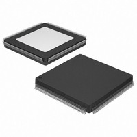
XC3S400-4PQ208C Xilinx Inc, XC3S400-4PQ208C Datasheet - Page 106

XC3S400-4PQ208C
Manufacturer Part Number
XC3S400-4PQ208C
Description
IC SPARTAN-3 FPGA 400K 208PQFP
Manufacturer
Xilinx Inc
Series
Spartan™-3r
Datasheet
1.XC3S50-4VQG100C.pdf
(217 pages)
Specifications of XC3S400-4PQ208C
Number Of Logic Elements/cells
8064
Number Of Labs/clbs
896
Total Ram Bits
294912
Number Of I /o
141
Number Of Gates
400000
Voltage - Supply
1.14 V ~ 1.26 V
Mounting Type
Surface Mount
Operating Temperature
0°C ~ 85°C
Package / Case
208-BFQFP
Other names
Q2844431
XC3S4004PQ208C
XC3S4004PQ208C
XC3S4004PQ208C
XC3S4004PQ208C
Available stocks
Company
Part Number
Manufacturer
Quantity
Price
Company:
Part Number:
XC3S400-4PQ208C
Manufacturer:
XILINX
Quantity:
392
Company:
Part Number:
XC3S400-4PQ208C
Manufacturer:
XILINX
Quantity:
5
Spartan-3 FPGA Family: Pinout Descriptions
Table 70: Dual-Purpose Pins Used in Master or Slave Serial Mode
Parallel Configuration Modes (SelectMAP)
This section describes the dual-purpose configuration pins
used during the Master and Slave Parallel configuration
modes, sometimes also called the SelectMAP modes. In
both Master and Slave Parallel configuration modes, D0-D7
form the byte-wide configuration data input. See
for Mode Select pin settings required for Parallel modes.
106
DIN
DOUT
INIT_B
Pin Name
Configuration Data Byte
Bidirectional
(open-drain)
Direction
Output
Input
0xFC =
Figure 39: Configuration Data Byte Mapping to D0-D7 Bits
Serial Data Input:
During the Master or Slave Serial configuration modes, DIN is the serial configuration data
input, and all data is synchronized to the rising CCLK edge. After configuration, this pin is
available as a user I/O.
This signal is located in Bank 4 and its output voltage determined by VCCO_4.
The BitGen option Persist permits this pin to retain its configuration function in the User
mode.
Serial Data Output:
In a multi-FPGA design where all the FPGAs use serial mode, connect the DOUT output of
one FPGA—in either Master or Slave Serial mode—to the DIN input of the next FPGA—in
Slave Serial mode—so that configuration data passes from one to the next, in daisy-chain
fashion. This “daisy chain” permits sequential configuration of multiple FPGAs.
This signal is located in Bank 4 and its output voltage determined by VCCO_4.
The BitGen option Persist permits this pin to retain its configuration function in the User
mode.
Initializing Configuration Memory/Configuration Error:
Just after power is applied, the FPGA produces a Low-to-High transition on this pin
indicating that initialization (i.e., clearing) of the configuration memory has finished. Before
entering the User mode, this pin functions as an open-drain output, which requires a pull-up
resistor in order to produce a High logic level. In a multi-FPGA design, tie (wire AND) the
INIT_B pins from all FPGAs together so that the common node transitions High only after
all of the FPGAs have been successfully initialized.
Externally holding this pin Low beyond the initialization phase delays the start of
configuration. This action stalls the FPGA at the configuration step just before the mode
select pins are sampled.
During configuration, the FPGA indicates the occurrence of a data (i.e., CRC) error by
asserting INIT_B Low.
This signal is located in Bank 4 and its output voltage determined by VCCO_4.
The BitGen option Persist permits this pin to retain its configuration function in the User
mode.
(MSB)
D0
1
I/O Bank 4 (VCCO_4)
Table 74
D1
High Nibble
1
www.xilinx.com
D2
1
As shown in
D7 is the least-significant bit. Bits D0-D3 form the high nib-
ble of the byte and bits D4-D7 form the low nibble.
In the Parallel configuration modes, both the VCCO_4 and
VCCO_5 voltage supplies are required and must both equal
the voltage of the attached configuration device, typically
either 2.5V or 3.3V.
D3
1
Description
Figure
D4
1
I/O Bank 5 (VCCO_5)
39, D0 is the most-significant bit while
D5
Low Nibble
1
DS099-4 (v2.5) December 4, 2009
D6
0
Product Specification
(LSB)
D7
0
R


