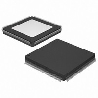
XC3S400-4PQ208C Xilinx Inc, XC3S400-4PQ208C Datasheet - Page 4

XC3S400-4PQ208C
Manufacturer Part Number
XC3S400-4PQ208C
Description
IC SPARTAN-3 FPGA 400K 208PQFP
Manufacturer
Xilinx Inc
Series
Spartan™-3r
Datasheet
1.XC3S50-4VQG100C.pdf
(217 pages)
Specifications of XC3S400-4PQ208C
Number Of Logic Elements/cells
8064
Number Of Labs/clbs
896
Total Ram Bits
294912
Number Of I /o
141
Number Of Gates
400000
Voltage - Supply
1.14 V ~ 1.26 V
Mounting Type
Surface Mount
Operating Temperature
0°C ~ 85°C
Package / Case
208-BFQFP
Other names
Q2844431
XC3S4004PQ208C
XC3S4004PQ208C
XC3S4004PQ208C
XC3S4004PQ208C
Available stocks
Company
Part Number
Manufacturer
Quantity
Price
Company:
Part Number:
XC3S400-4PQ208C
Manufacturer:
XILINX
Quantity:
392
Company:
Part Number:
XC3S400-4PQ208C
Manufacturer:
XILINX
Quantity:
5
- Current page: 4 of 217
- Download datasheet (6Mb)
Spartan-3 FPGA Family: Introduction and Ordering Information
Architectural Overview
The Spartan-3 family architecture consists of five funda-
mental programmable functional elements:
•
•
•
•
4
10
Configurable Logic Blocks (CLBs) contain RAM-based
Look-Up Tables (LUTs) to implement logic and storage
elements that can be used as flip-flops or latches.
CLBs can be programmed to perform a wide variety of
logical functions as well as to store data.
Input/Output Blocks (IOBs) control the flow of data
between the I/O pins and the internal logic of the
device. Each IOB supports bidirectional data flow plus
3-state operation. Twenty-six different signal standards,
including eight high-performance differential standards,
are available as shown in
(DDR) registers are included. The Digitally Controlled
Impedance (DCI) feature provides automatic on-chip
terminations, simplifying board designs.
Block RAM provides data storage in the form of 18-Kbit
dual-port blocks.
Multiplier blocks accept two 18-bit binary numbers as
inputs and calculate the product.
Notes:
1.
The two additional block RAM columns of the XC3S4000 and XC3S5000
devices are shown with dashed lines. The XC3S50 has only the block RAM
column on the far left.
Table
2. Double Data-Rate
Figure 1: Spartan-3 Family Architecture
www.xilinx.com
•
These elements are organized as shown in
of IOBs surrounds a regular array of CLBs. The XC3S50
has a single column of block RAM embedded in the array.
Those devices ranging from the XC3S200 to the XC3S2000
have two columns of block RAM. The XC3S4000 and
XC3S5000 devices have four RAM columns. Each column
is made up of several 18-Kbit RAM blocks; each block is
associated with a dedicated multiplier. The DCMs are posi-
tioned at the ends of the outer block RAM columns.
The Spartan-3 family features a rich network of traces and
switches that interconnect all five functional elements,
transmitting signals among them. Each functional element
has an associated switch matrix that permits multiple con-
nections to the routing.
Digital
self-calibrating, fully digital solutions for distributing,
delaying, multiplying, dividing, and phase shifting clock
signals.
Clock
Manager
DS099-1_01_032703
DS099-1 (v2.5) December 4, 2009
(DCM)
Product Specification
blocks
Figure
1. A ring
provide
R
Related parts for XC3S400-4PQ208C
Image
Part Number
Description
Manufacturer
Datasheet
Request
R

Part Number:
Description:
SPARTAN-3A FPGA 400K 208-PQFP
Manufacturer:
Xilinx Inc
Datasheet:

Part Number:
Description:
SPARTAN-3A FPGA 400K 256-FTBGA
Manufacturer:
Xilinx Inc
Datasheet:

Part Number:
Description:
SPARTAN3A FPGA 400K STD 256FTBGA
Manufacturer:
Xilinx Inc

Part Number:
Description:
IC SPARTAN-3 FPGA 400K 320-FBGA
Manufacturer:
Xilinx Inc
Datasheet:

Part Number:
Description:
SEMI CONDUCTOR
Manufacturer:
Xilinx Inc
Datasheet:

Part Number:
Description:
FPGA Spartan®-3 Family 400K Gates 8064 Cells 630MHz 90nm Technology 1.2V 456-Pin FBGA
Manufacturer:
Xilinx Inc
Datasheet:

Part Number:
Description:
FPGA Spartan®-3 Family 400K Gates 8064 Cells 630MHz 90nm Technology 1.2V 320-Pin FBGA
Manufacturer:
Xilinx Inc
Datasheet:

Part Number:
Description:
FPGA Spartan®-3 Family 400K Gates 8064 Cells 630MHz 90nm Technology 1.2V 456-Pin FBGA
Manufacturer:
Xilinx Inc
Datasheet:

Part Number:
Description:
FPGA Spartan®-3 Family 400K Gates 8064 Cells 630MHz 90nm Technology 1.2V 256-Pin FTBGA
Manufacturer:
Xilinx Inc
Datasheet:

Part Number:
Description:
FPGA Spartan®-3 Family 400K Gates 8064 Cells 630MHz 90nm Technology 1.2V 208-Pin PQFP
Manufacturer:
Xilinx Inc
Datasheet:

Part Number:
Description:
FPGA Spartan®-3 Family 400K Gates 8064 Cells 630MHz 90nm Technology 1.2V 144-Pin TQFP
Manufacturer:
Xilinx Inc
Datasheet:

Part Number:
Description:
FPGA Spartan®-3 Family 400K Gates 8064 Cells 630MHz 90nm Technology 1.2V 144-Pin TQFP
Manufacturer:
Xilinx Inc
Datasheet:

Part Number:
Description:
FPGA Spartan®-3 Family 400K Gates 8064 Cells 725MHz 90nm Technology 1.2V 256-Pin FTBGA
Manufacturer:
Xilinx Inc
Datasheet:

Part Number:
Description:
FPGA Spartan®-3 Family 400K Gates 8064 Cells 630MHz 90nm Technology 1.2V 456-Pin FBGA
Manufacturer:
Xilinx Inc
Datasheet:

Part Number:
Description:
FPGA Spartan®-3 Family 400K Gates 8064 Cells 630MHz 90nm Technology 1.2V 320-Pin FBGA
Manufacturer:
Xilinx Inc
Datasheet:


