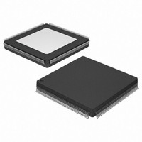
XC3S400-4PQ208C Xilinx Inc, XC3S400-4PQ208C Datasheet - Page 69

XC3S400-4PQ208C
Manufacturer Part Number
XC3S400-4PQ208C
Description
IC SPARTAN-3 FPGA 400K 208PQFP
Manufacturer
Xilinx Inc
Series
Spartan™-3r
Datasheet
1.XC3S50-4VQG100C.pdf
(217 pages)
Specifications of XC3S400-4PQ208C
Number Of Logic Elements/cells
8064
Number Of Labs/clbs
896
Total Ram Bits
294912
Number Of I /o
141
Number Of Gates
400000
Voltage - Supply
1.14 V ~ 1.26 V
Mounting Type
Surface Mount
Operating Temperature
0°C ~ 85°C
Package / Case
208-BFQFP
Other names
Q2844431
XC3S4004PQ208C
XC3S4004PQ208C
XC3S4004PQ208C
XC3S4004PQ208C
Available stocks
Company
Part Number
Manufacturer
Quantity
Price
Company:
Part Number:
XC3S400-4PQ208C
Manufacturer:
XILINX
Quantity:
392
Company:
Part Number:
XC3S400-4PQ208C
Manufacturer:
XILINX
Quantity:
5
- Current page: 69 of 217
- Download datasheet (6Mb)
Table 41: Setup and Hold Times for the IOB Input Path
DS099-3 (v2.5) December 4, 2009
Product Specification
98
Notes:
1.
2.
3.
Setup Times
Hold Times
Set/Reset Pulse Width
T
The numbers in this table are tested using the methodology presented in
Table 31
This setup time requires adjustment whenever a signal standard other than LVCMOS25 is assigned to the data Input. If this is true, add the
appropriate Input adjustment from
These hold times require adjustment whenever a signal standard other than LVCMOS25 is assigned to the data Input. If this is true, subtract
the appropriate Input adjustment from
edge.
T
T
Symbol
T
T
RPW_IOB
IOPICKD
IOICKPD
IOPICK
IOICKP
R
and
Table
Time from the setup of data at the Input
pin to the active transition at the ICLK
input of the Input Flip-Flop (IFF). No Input
Delay is programmed.
Time from the setup of data at the Input
pin to the active transition at the IFF’s
ICLK input. The Input Delay is
programmed.
Time from the active transition at the IFF’s
ICLK input to the point where data must
be held at the Input pin. No Input Delay is
programmed.
Time from the active transition at the IFF’s
ICLK input to the point where data must
be held at the Input pin. The Input Delay
is programmed.
Minimum pulse width to SR control input
on IOB
34.
Description
Table
Table
43.
43. When the hold time is negative, it is possible to change the data before the clock’s active
Spartan-3 FPGA Family: DC and Switching Characteristics
www.xilinx.com
LVCMOS25
IOBDELAY = NONE
LVCMOS25
IOBDELAY = IFD
LVCMOS25
IOBDELAY = NONE
LVCMOS25
IOBDELAY = IFD
Conditions
(2)
(2)
(2)
(2)
Table 47
,
,
,
,
and are based on the operating conditions set forth in
XC3S50
XC3S200
XC3S400
XC3S1000
XC3S1500
XC3S2000
XC3S4000
XC3S5000
XC3S50
XC3S200
XC3S400
XC3S1000
XC3S1500
XC3S2000
XC3S4000
XC3S5000
XC3S50
XC3S200
XC3S400
XC3S1000
XC3S1500
XC3S2000
XC3S4000
XC3S5000
XC3S50
XC3S200
XC3S400
XC3S1000
XC3S1500
XC3S2000
XC3S4000
XC3S5000
Device
All
-0.55
-0.29
-0.29
-0.55
-0.55
-0.55
-0.61
-0.68
-2.74
-3.00
-2.90
-3.24
-3.55
-4.57
-4.96
-5.09
1.65
1.37
1.37
1.65
1.65
1.65
1.73
1.82
4.39
4.76
4.63
5.02
5.40
6.68
7.16
7.33
0.66
Min
-5
Speed Grade
-0.55
-0.55
-0.55
-0.55
-0.61
-0.68
-2.74
-3.24
-3.55
-4.57
-4.96
-5.09
-0.29
-0.29
-3.00
-2.90
1.89
1.57
1.57
1.89
1.89
1.89
1.99
2.09
5.04
5.47
5.32
5.76
6.20
7.68
8.24
8.42
0.76
Min
-4
Units
ns
ns
ns
ns
ns
ns
ns
ns
ns
ns
ns
ns
ns
ns
ns
ns
ns
ns
ns
ns
ns
ns
ns
ns
ns
ns
ns
ns
ns
ns
ns
ns
ns
69
Related parts for XC3S400-4PQ208C
Image
Part Number
Description
Manufacturer
Datasheet
Request
R

Part Number:
Description:
SPARTAN-3A FPGA 400K 208-PQFP
Manufacturer:
Xilinx Inc
Datasheet:

Part Number:
Description:
SPARTAN-3A FPGA 400K 256-FTBGA
Manufacturer:
Xilinx Inc
Datasheet:

Part Number:
Description:
SPARTAN3A FPGA 400K STD 256FTBGA
Manufacturer:
Xilinx Inc

Part Number:
Description:
IC SPARTAN-3 FPGA 400K 320-FBGA
Manufacturer:
Xilinx Inc
Datasheet:

Part Number:
Description:
SEMI CONDUCTOR
Manufacturer:
Xilinx Inc
Datasheet:

Part Number:
Description:
FPGA Spartan®-3 Family 400K Gates 8064 Cells 630MHz 90nm Technology 1.2V 456-Pin FBGA
Manufacturer:
Xilinx Inc
Datasheet:

Part Number:
Description:
FPGA Spartan®-3 Family 400K Gates 8064 Cells 630MHz 90nm Technology 1.2V 320-Pin FBGA
Manufacturer:
Xilinx Inc
Datasheet:

Part Number:
Description:
FPGA Spartan®-3 Family 400K Gates 8064 Cells 630MHz 90nm Technology 1.2V 456-Pin FBGA
Manufacturer:
Xilinx Inc
Datasheet:

Part Number:
Description:
FPGA Spartan®-3 Family 400K Gates 8064 Cells 630MHz 90nm Technology 1.2V 256-Pin FTBGA
Manufacturer:
Xilinx Inc
Datasheet:

Part Number:
Description:
FPGA Spartan®-3 Family 400K Gates 8064 Cells 630MHz 90nm Technology 1.2V 208-Pin PQFP
Manufacturer:
Xilinx Inc
Datasheet:

Part Number:
Description:
FPGA Spartan®-3 Family 400K Gates 8064 Cells 630MHz 90nm Technology 1.2V 144-Pin TQFP
Manufacturer:
Xilinx Inc
Datasheet:

Part Number:
Description:
FPGA Spartan®-3 Family 400K Gates 8064 Cells 630MHz 90nm Technology 1.2V 144-Pin TQFP
Manufacturer:
Xilinx Inc
Datasheet:

Part Number:
Description:
FPGA Spartan®-3 Family 400K Gates 8064 Cells 725MHz 90nm Technology 1.2V 256-Pin FTBGA
Manufacturer:
Xilinx Inc
Datasheet:

Part Number:
Description:
FPGA Spartan®-3 Family 400K Gates 8064 Cells 630MHz 90nm Technology 1.2V 456-Pin FBGA
Manufacturer:
Xilinx Inc
Datasheet:

Part Number:
Description:
FPGA Spartan®-3 Family 400K Gates 8064 Cells 630MHz 90nm Technology 1.2V 320-Pin FBGA
Manufacturer:
Xilinx Inc
Datasheet:


