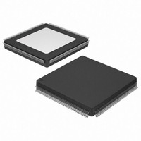
XC3S400-4PQ208C Xilinx Inc, XC3S400-4PQ208C Datasheet - Page 42

XC3S400-4PQ208C
Manufacturer Part Number
XC3S400-4PQ208C
Description
IC SPARTAN-3 FPGA 400K 208PQFP
Manufacturer
Xilinx Inc
Series
Spartan™-3r
Datasheet
1.XC3S50-4VQG100C.pdf
(217 pages)
Specifications of XC3S400-4PQ208C
Number Of Logic Elements/cells
8064
Number Of Labs/clbs
896
Total Ram Bits
294912
Number Of I /o
141
Number Of Gates
400000
Voltage - Supply
1.14 V ~ 1.26 V
Mounting Type
Surface Mount
Operating Temperature
0°C ~ 85°C
Package / Case
208-BFQFP
Other names
Q2844431
XC3S4004PQ208C
XC3S4004PQ208C
XC3S4004PQ208C
XC3S4004PQ208C
Available stocks
Company
Part Number
Manufacturer
Quantity
Price
Company:
Part Number:
XC3S400-4PQ208C
Manufacturer:
XILINX
Quantity:
392
Company:
Part Number:
XC3S400-4PQ208C
Manufacturer:
XILINX
Quantity:
5
- Current page: 42 of 217
- Download datasheet (6Mb)
Spartan-3 FPGA Family: Functional Description
Table 24: BUFGMUX Select Mechanism
The two clock inputs can be asynchronous with regard to
each other, and the S input can change at any time, except
for a short setup time prior to the rising edge of the presently
selected clock (I0 or I1). Violating this setup time require-
ment can result in an undefined runt pulse output.
The BUFG clock buffer primitive drives a single clock signal
onto the clock network and is essentially the same element
as a BUFGMUX, just without the clock select mechanism.
Similarly, the BUFGCE primitive creates an enabled clock
buffer using the BUFGMUX select mechanism.
Each BUFGMUX buffers incoming clock signals to two pos-
sible destinations:
1. The vertical spine belonging to the same side of the die
42
54
— top or bottom — as the BUFGMUX element in use.
The two spines — top and bottom — each comprise
four vertical clock lines, each running from one of the
BUFGMUX elements on the same side towards the
center of the die. At the center of the die, clock signals
S Input
0
1
O Output
I0 Input
I1 Input
www.xilinx.com
2. The clock input of either DCM on the same side of the
Use either a BUFGMUX element or a BUFG (Global Clock
Buffer) element to place a Global input in the design. For the
purpose of minimizing the dynamic power dissipation of the
clock network, the Xilinx development software automati-
cally disables all clock line segments that a design does not
use.
A global clock line ideally drives clock inputs on the various
clocked elements within the FPGA, such as CLB or IOB
flip-flops or block RAMs. A global clock line also optionally
drives combinatorial inputs. However, doing so provides
additional loading on the clock line that might also affect
clock jitter. Ideally, drive combinatorial inputs using the sig-
nal that also drives the input to the BUFGMUX or BUFG ele-
ment.
For more details, refer to the “Using Global Clock
Resources” chapter in UG331.
reach the eight-line horizontal spine, which spans the
width of the die. In turn, the horizontal spine branches
out into a subsidiary clock interconnect that accesses
the CLBs.
die — top or bottom — as the BUFGMUX element in
use.
DS099-2 (v2.5) December 4, 2009
Product Specification
R
Related parts for XC3S400-4PQ208C
Image
Part Number
Description
Manufacturer
Datasheet
Request
R

Part Number:
Description:
SPARTAN-3A FPGA 400K 208-PQFP
Manufacturer:
Xilinx Inc
Datasheet:

Part Number:
Description:
SPARTAN-3A FPGA 400K 256-FTBGA
Manufacturer:
Xilinx Inc
Datasheet:

Part Number:
Description:
SPARTAN3A FPGA 400K STD 256FTBGA
Manufacturer:
Xilinx Inc

Part Number:
Description:
IC SPARTAN-3 FPGA 400K 320-FBGA
Manufacturer:
Xilinx Inc
Datasheet:

Part Number:
Description:
SEMI CONDUCTOR
Manufacturer:
Xilinx Inc
Datasheet:

Part Number:
Description:
FPGA Spartan®-3 Family 400K Gates 8064 Cells 630MHz 90nm Technology 1.2V 456-Pin FBGA
Manufacturer:
Xilinx Inc
Datasheet:

Part Number:
Description:
FPGA Spartan®-3 Family 400K Gates 8064 Cells 630MHz 90nm Technology 1.2V 320-Pin FBGA
Manufacturer:
Xilinx Inc
Datasheet:

Part Number:
Description:
FPGA Spartan®-3 Family 400K Gates 8064 Cells 630MHz 90nm Technology 1.2V 456-Pin FBGA
Manufacturer:
Xilinx Inc
Datasheet:

Part Number:
Description:
FPGA Spartan®-3 Family 400K Gates 8064 Cells 630MHz 90nm Technology 1.2V 256-Pin FTBGA
Manufacturer:
Xilinx Inc
Datasheet:

Part Number:
Description:
FPGA Spartan®-3 Family 400K Gates 8064 Cells 630MHz 90nm Technology 1.2V 208-Pin PQFP
Manufacturer:
Xilinx Inc
Datasheet:

Part Number:
Description:
FPGA Spartan®-3 Family 400K Gates 8064 Cells 630MHz 90nm Technology 1.2V 144-Pin TQFP
Manufacturer:
Xilinx Inc
Datasheet:

Part Number:
Description:
FPGA Spartan®-3 Family 400K Gates 8064 Cells 630MHz 90nm Technology 1.2V 144-Pin TQFP
Manufacturer:
Xilinx Inc
Datasheet:

Part Number:
Description:
FPGA Spartan®-3 Family 400K Gates 8064 Cells 725MHz 90nm Technology 1.2V 256-Pin FTBGA
Manufacturer:
Xilinx Inc
Datasheet:

Part Number:
Description:
FPGA Spartan®-3 Family 400K Gates 8064 Cells 630MHz 90nm Technology 1.2V 456-Pin FBGA
Manufacturer:
Xilinx Inc
Datasheet:

Part Number:
Description:
FPGA Spartan®-3 Family 400K Gates 8064 Cells 630MHz 90nm Technology 1.2V 320-Pin FBGA
Manufacturer:
Xilinx Inc
Datasheet:


