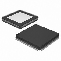
XC3S400-4PQ208C Xilinx Inc, XC3S400-4PQ208C Datasheet - Page 58

XC3S400-4PQ208C
Manufacturer Part Number
XC3S400-4PQ208C
Description
IC SPARTAN-3 FPGA 400K 208PQFP
Manufacturer
Xilinx Inc
Series
Spartan™-3r
Datasheet
1.XC3S50-4VQG100C.pdf
(217 pages)
Specifications of XC3S400-4PQ208C
Number Of Logic Elements/cells
8064
Number Of Labs/clbs
896
Total Ram Bits
294912
Number Of I /o
141
Number Of Gates
400000
Voltage - Supply
1.14 V ~ 1.26 V
Mounting Type
Surface Mount
Operating Temperature
0°C ~ 85°C
Package / Case
208-BFQFP
Other names
Q2844431
XC3S4004PQ208C
XC3S4004PQ208C
XC3S4004PQ208C
XC3S4004PQ208C
Available stocks
Company
Part Number
Manufacturer
Quantity
Price
Company:
Part Number:
XC3S400-4PQ208C
Manufacturer:
XILINX
Quantity:
392
Company:
Part Number:
XC3S400-4PQ208C
Manufacturer:
XILINX
Quantity:
5
Spartan-3 FPGA Family: DC and Switching Characteristics
Table 31: General Recommended Operating Conditions
Table 32: General DC Characteristics of User I/O, Dual-Purpose, and Dedicated Pins
58
Notes:
1.
2.
3.
4.
5.
6.
Symbol
I
I
R
RPU
RPD
I
PU
L
The V
range specific to each of the single-ended I/O standards is given in
Table
Only during DCM operation is it recommended that the rate of change of V
Input voltages outside the recommended range are permissible provided that the I
Table
Each of the User I/O and Dual-Purpose pins is associated with one of the V
diode junctions that exist between these pins and their associated V
is provided in
All Dedicated pins (PROG_B, DONE, TCK, TDI, TDO, and TMS) draw power from the V
ensures that the internal diode junctions that exist between each of these pins and the V
See XAPP459, “Eliminating I/O Coupling Effects when Interfacing Large-Swing Single-Ended Signals to User I/O Pins.”
ΔV
(2)
V
(3)
V
(3)
(3)
Symbol
V
CCAUX
V
CCO
CCAUX
CCINT
IN
T
CCO
36.
27.
J
(3)
Leakage current at User I/O,
Dual-Purpose, and Dedicated pins
Current through pull-up resistor at User
I/O, Dual-Purpose, and Dedicated pins
Equivalent resistance of pull-up resistor at
User I/O, Dual-Purpose, and Dedicated
pins, derived from I
Current through pull-down resistor at User
I/O, Dual-Purpose, and Dedicated pins
(1)
(2)
range given here spans the lowest and highest operating voltages of all supported I/O standards. The recommended V
Table
Junction temperature
Internal supply voltage
Output driver supply voltage
Auxiliary supply voltage
Voltage variance on V
Voltage applied to all User
I/O pins and Dual-Purpose
pins relative to GND
Voltage applied to all
Dedicated pins relative to
GND
27.
Description
(5)
RPU
Description
(4, 6)
CCAUX
when using a DCM
Driver is Hi-Z, V
Commercial
Industrial
V
V
0V or V
www.xilinx.com
CCO
CCO
sample-tested
V
V
V
V
V
V
V
= 3.3V
≤ 2.5V
V
V
V
V
CCO
IN
IN
IN
IN
IN
IN
CCO
CCO
CCO
CCO
CCO
Test Conditions
= 0V, V
= 0V, V
= 0V, V
= 0V, V
= 0V, V
= 0V, V
V
= 3.0V to 3.465V
max,
= 1.14 to 1.26V
Table
IN
CCO
= 2.3V to 2.7V
= 1.7V to 1.9V
= 1.4V to 1.6V
IN
= V
=
CCO
CCO
CCO
CCO
CCO
CCO
and GND rails do not turn on. The absolute maximum rating
34, and that specific to the differential standards is given in
CCO
CCAUX
CCO
= 3.3V
= 3.0V
= 2.5V
= 1.8V
= 1.5V
= 1.2V
V
V
CCO
CCO
1.140
1.140
2.375
–0.3
–0.3
–0.3
Min
–40
rails. Meeting the V
0
-
not exceed 10 mV/ms.
> 3.0V
< 3.0V
IK
input diode clamp diode rating is met. Refer to
CCAUX
CCAUX
1.200
2.500
Nom
25
25
–0.84
–0.69
–0.47
–0.21
–0.13
–0.06
-
-
-
-
-
1.27
1.15
2.45
3.25
5.15
0.37
rail (2.5V). Meeting the V
Min
and GND rails do not turn on.
-
-
DS099-3 (v2.5) December 4, 2009
IN
V
limit ensures that the internal
V
CCAUX
CCO
Typ
-
-
-
-
-
-
-
-
-
-
-
-
-
-
1.260
3.465
2.625
3.75
Max
100
85
10
Product Specification
+ 0.3
+ 0.3
–2.35
–1.99
–1.41
–0.69
–0.43
–0.22
12.10
21.00
Max
4.11
3.25
9.10
1.67
±
±
(4)
(5)
25
10
IN
mV/ms
max limit
Units
Units
° C
° C
V
V
V
V
V
V
mA
mA
mA
mA
mA
mA
mA
μA
μA
kΩ
kΩ
kΩ
kΩ
kΩ
CCO
R


