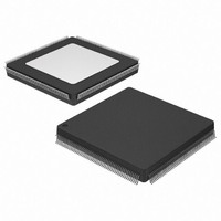
XC3S400-4PQ208C Xilinx Inc, XC3S400-4PQ208C Datasheet - Page 65

XC3S400-4PQ208C
Manufacturer Part Number
XC3S400-4PQ208C
Description
IC SPARTAN-3 FPGA 400K 208PQFP
Manufacturer
Xilinx Inc
Series
Spartan™-3r
Datasheet
1.XC3S50-4VQG100C.pdf
(217 pages)
Specifications of XC3S400-4PQ208C
Number Of Logic Elements/cells
8064
Number Of Labs/clbs
896
Total Ram Bits
294912
Number Of I /o
141
Number Of Gates
400000
Voltage - Supply
1.14 V ~ 1.26 V
Mounting Type
Surface Mount
Operating Temperature
0°C ~ 85°C
Package / Case
208-BFQFP
Other names
Q2844431
XC3S4004PQ208C
XC3S4004PQ208C
XC3S4004PQ208C
XC3S4004PQ208C
Available stocks
Company
Part Number
Manufacturer
Quantity
Price
Company:
Part Number:
XC3S400-4PQ208C
Manufacturer:
XILINX
Quantity:
392
Company:
Part Number:
XC3S400-4PQ208C
Manufacturer:
XILINX
Quantity:
5
- Current page: 65 of 217
- Download datasheet (6Mb)
Table 37: DC Characteristics of User I/Os Using Differential Signal Standards
DS099-3 (v2.5) December 4, 2009
Product Specification
98
Notes:
1.
2.
3.
4.
5.
6.
LDT_25 (ULVDS_25)
LVDS_25
BLVDS_25
LVDSEXT_25
LVPECL_25
RSDS_25
DIFF_HSTL_II_18
DIFF_SSTL2_II
Signal Standard
Mask revision E devices have tighter output ranges but can be used in any design that was in a previous revision. See
Revisions, page
The numbers in this table are based on the conditions set forth in
This value must be compatible with the receiver to which the FPGA’s output pair is connected.
Output voltage measurements for all differential standards are made with a termination resistor (R
of the differential signal pair.
Only one of the differential standards RSDS_25, LDT_25, LVDS_25, and LVDSEXT_25 may be used for outputs within a bank.
Each differential standard input-pair requires an external 100Ω termination resistor.
Each LVPECL_25 or BLVDS_25 output-pair requires three external resistors for proper output operation as shown in
LVPECL_25 or BLVDS_25 input-pair uses a 100Ω termination resistor at the receiver.
(5)
(6)
(6)
R
LVPECL
Figure 32: External Termination Required for LVPECL and BLVDS Output and Input
55.
70Ω
70Ω
Revision
Mask
All
All
‘E’
All
All
‘E’
All
All
‘E’
All
All
Internal
GND level
Logic
240Ω
(1)
V
V
OUTN
OUTP
Z
Z
0
0
=50Ω
Min (mV) Typ (mV)
=50Ω
430
100
200
250
100
300
100
200
V
-
-
-
OCM
V
V
V
(3)
Figure 31: Differential Output Voltages
OD
OH
OL
50%
= Output common mode voltage =
= Output differential voltage =
= Output voltage indicating a Low logic level
= Output voltage indicating a High logic level
100Ω
Spartan-3 FPGA Family: DC and Switching Characteristics
600
350
V
-
-
-
-
-
-
-
-
-
OD
V
LVPECL
OCM
www.xilinx.com
Max (mV)
670
600
500
450
600
700
600
500
-
-
-
V
V
Table 31
OUTP
V
BLVDS
OD
OUTN
Min (V)
0.495
V
0.80
0.80
0.80
1.0
1.0
1.0
V
OUTP
and
-
-
-
-
OH
165Ω
165Ω
N
P
V
OUTP
Table
- V
OUTN
Differential
I/O Pair Pins
Typ (V)
2
V
+ V
0.600
1.20
OCM
36.
140Ω
V
-
-
-
-
-
-
-
-
-
OUTN
OL
DS099-3_02_012304
Z
Z
0
0
=50Ω
=50Ω
Max (V)
0.715
1.6
1.5
1.6
1.5
1.6
1.5
T
-
-
-
-
) of 100Ω across the N and P pins
100Ω
V
V
CCO
Min (V)
TT
ds099-3_08_112105
0.71
0.85
0.85
1.35
0.85
V
1.10
1.15
1.10
BLVDS
+ 0.80
OH
-
– 0.40
Figure
Mask and Fab
V
Max (V)
TT
1.005
32. Each
0.50
1.55
1.40
1.55
1.35
1.55
1.40
0.40
V
– 0.80
OL
-
65
Related parts for XC3S400-4PQ208C
Image
Part Number
Description
Manufacturer
Datasheet
Request
R

Part Number:
Description:
SPARTAN-3A FPGA 400K 208-PQFP
Manufacturer:
Xilinx Inc
Datasheet:

Part Number:
Description:
SPARTAN-3A FPGA 400K 256-FTBGA
Manufacturer:
Xilinx Inc
Datasheet:

Part Number:
Description:
SPARTAN3A FPGA 400K STD 256FTBGA
Manufacturer:
Xilinx Inc

Part Number:
Description:
IC SPARTAN-3 FPGA 400K 320-FBGA
Manufacturer:
Xilinx Inc
Datasheet:

Part Number:
Description:
SEMI CONDUCTOR
Manufacturer:
Xilinx Inc
Datasheet:

Part Number:
Description:
FPGA Spartan®-3 Family 400K Gates 8064 Cells 630MHz 90nm Technology 1.2V 456-Pin FBGA
Manufacturer:
Xilinx Inc
Datasheet:

Part Number:
Description:
FPGA Spartan®-3 Family 400K Gates 8064 Cells 630MHz 90nm Technology 1.2V 320-Pin FBGA
Manufacturer:
Xilinx Inc
Datasheet:

Part Number:
Description:
FPGA Spartan®-3 Family 400K Gates 8064 Cells 630MHz 90nm Technology 1.2V 456-Pin FBGA
Manufacturer:
Xilinx Inc
Datasheet:

Part Number:
Description:
FPGA Spartan®-3 Family 400K Gates 8064 Cells 630MHz 90nm Technology 1.2V 256-Pin FTBGA
Manufacturer:
Xilinx Inc
Datasheet:

Part Number:
Description:
FPGA Spartan®-3 Family 400K Gates 8064 Cells 630MHz 90nm Technology 1.2V 208-Pin PQFP
Manufacturer:
Xilinx Inc
Datasheet:

Part Number:
Description:
FPGA Spartan®-3 Family 400K Gates 8064 Cells 630MHz 90nm Technology 1.2V 144-Pin TQFP
Manufacturer:
Xilinx Inc
Datasheet:

Part Number:
Description:
FPGA Spartan®-3 Family 400K Gates 8064 Cells 630MHz 90nm Technology 1.2V 144-Pin TQFP
Manufacturer:
Xilinx Inc
Datasheet:

Part Number:
Description:
FPGA Spartan®-3 Family 400K Gates 8064 Cells 725MHz 90nm Technology 1.2V 256-Pin FTBGA
Manufacturer:
Xilinx Inc
Datasheet:

Part Number:
Description:
FPGA Spartan®-3 Family 400K Gates 8064 Cells 630MHz 90nm Technology 1.2V 456-Pin FBGA
Manufacturer:
Xilinx Inc
Datasheet:

Part Number:
Description:
FPGA Spartan®-3 Family 400K Gates 8064 Cells 630MHz 90nm Technology 1.2V 320-Pin FBGA
Manufacturer:
Xilinx Inc
Datasheet:


