CY7C67300-100AXI Cypress Semiconductor Corp, CY7C67300-100AXI Datasheet - Page 58
CY7C67300-100AXI
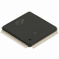
Manufacturer Part Number
CY7C67300-100AXI
Description
IC USB HOST/PERIPH CNTRL 100LQFP
Manufacturer
Cypress Semiconductor Corp
Series
EZ-Host™r
Type
Host Programmable Embedded USBr
Datasheet
1.CY7C67300-100AXI.pdf
(99 pages)
Specifications of CY7C67300-100AXI
Package / Case
100-LQFP
Applications
USB Host/Peripheral Controller
Core Processor
CY16
Program Memory Type
ROM (8 kB)
Controller Series
CY7C673xx
Ram Size
16K x 8
Interface
SPI Serial, USB, HPI
Number Of I /o
32
Voltage - Supply
3 V ~ 3.6 V
Operating Temperature
-40°C ~ 85°C
Mounting Type
Surface Mount
Maximum Operating Temperature
+ 85 C
Minimum Operating Temperature
- 40 C
Mounting Style
SMD/SMT
Operating Temperature Range
- 40 C to + 85 C
Supply Current
80 mA
Operating Supply Voltage
3.3 V
Lead Free Status / RoHS Status
Lead free / RoHS Compliant
For Use With
CY4640 - KIT MASS STORAGE REF DESIGNCY3663 - KIT DEV EZ-OTG/EZ-HOST
Lead Free Status / Rohs Status
Lead free / RoHS Compliant
Other names
428-1865
CY7C67300-100AXI
CY7C67300-100AXI
Available stocks
Company
Part Number
Manufacturer
Quantity
Price
Company:

Part Number:
CY7C67300-100AXI
Manufacturer:
ATMEL
Quantity:
210
Company:
Part Number:
CY7C67300-100AXI
Manufacturer:
CYPRESS
Quantity:
246
Company:
Part Number:
CY7C67300-100AXI
Manufacturer:
Cypress Semiconductor Corp
Quantity:
10 000
Part Number:
CY7C67300-100AXI
Manufacturer:
CYPRESS
Quantity:
20 000
Company:
Part Number:
CY7C67300-100AXIT
Manufacturer:
Cypress Semiconductor Corp
Quantity:
10 000


HSS Transmit Gap Register [0xC074] [R/W]
Table 92. HSS Transmit Gap Register
Register Description
The HSS Transmit Gap register is only valid in block transmit
mode. It allows for a programmable number of stop bits to be
inserted, thus overwriting the One Stop Bit in the HSS Control
register. The default reset value of this register is 0x0009, equiv-
alent to two stop bits.
Transmit Gap Select (Bits [7:0])
The Transmit Gap Select field sets the inactive time between
transmitted bytes. The inactive time = (Transmit Gap Select –7)
* bit time. Therefore a Transmit Gap Select Value of 8 is equal to
having one Stop bit.
HSS Data Register [0xC076] [R/W]
Table 93. HSS Data Register
Register Description
The HSS Data register contains data received on the HSS port
(not for block receive mode) when read. This receive data is valid
when the Receive Ready bit of the HSS Control register is set to
‘1’. Writing to this register initiates a single byte transfer of data.
The Transmit Ready Flag in the HSS Control register must read
‘1’ before writing to this register (this avoids disrupting the
previous/current transmission).
Document #: 38-08015 Rev. *J
Bit #
Field
Read/Write
Default
Bit #
Field
Read/Write
Default
Bit #
Field
Read/Write
Default
Bit #
Field
Read/Write
Default
R/W
R/W
15
15
X
X
0
7
0
7
-
-
R/W
R/W
14
14
X
X
0
6
0
6
-
-
R/W
R/W
13
13
X
X
0
5
0
5
-
-
Transmit Gap Select
R/W
R/W
12
12
X
X
0
4
0
4
-
-
Reserved
Reserved
Reserved
Write all reserved bits with ’0’.
Data (Bits [7:0])
The Data field contains the data received or to be transmitted on
the HSS port.
Reserved
Write all reserved bits with ’0’.
Data
R/W
R/W
11
11
0
X
X
3
1
3
-
-
R/W
R/W
10
10
0
X
X
2
0
2
-
-
R/W
R/W
9
0
X
X
1
0
9
1
-
-
CY7C67300
Page 58 of 99
R/W
R/W
8
0
X
X
-
0
1
8
0
-
[+] Feedback
Related parts for CY7C67300-100AXI
Image
Part Number
Description
Manufacturer
Datasheet
Request
R

Part Number:
Description:
Manufacturer:
Cypress Semiconductor Corp
Datasheet:

Part Number:
Description:
IC USB HOST/PERIPH CNTRL 100LQFP
Manufacturer:
Cypress Semiconductor Corp
Datasheet:
Part Number:
Description:
IC,Peripheral (Multifunction) Controller,QFP,100PIN
Manufacturer:
Cypress Semiconductor Corp
Datasheet:
Part Number:
Description:
IC,Peripheral (Multifunction) Controller,QFP,100PIN
Manufacturer:
Cypress Semiconductor Corp
Datasheet:
Part Number:
Description:
IC,Peripheral (Multifunction) Controller,QFP,100PIN
Manufacturer:
Cypress Semiconductor Corp
Datasheet:
Part Number:
Description:
Manufacturer:
Cypress Semiconductor Corp
Datasheet:
Part Number:
Description:
Manufacturer:
Cypress Semiconductor Corp
Datasheet:
Part Number:
Description:
Manufacturer:
Cypress Semiconductor Corp
Datasheet: