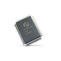
PI7C7300DNAE Pericom Semiconductor, PI7C7300DNAE Datasheet - Page 100

PI7C7300DNAE
Manufacturer Part Number
PI7C7300DNAE
Description
IC PCI-PCI BRIDGE 3PORT 272-BGA
Manufacturer
Pericom Semiconductor
Datasheet
1.PI7C7300DNAE.pdf
(107 pages)
Specifications of PI7C7300DNAE
Applications
*
Interface
*
Voltage - Supply
*
Package / Case
272-PBGA
Mounting Type
Surface Mount
Maximum Operating Temperature
+ 85 C
Minimum Operating Temperature
- 40 C
Mounting Style
SMD/SMT
Operating Supply Voltage
3 V to 3.6 V
Supply Current (max)
660 mA
Lead Free Status / RoHS Status
Lead free / RoHS Compliant
Available stocks
Company
Part Number
Manufacturer
Quantity
Price
Company:
Part Number:
PI7C7300DNAE
Manufacturer:
Pericom
Quantity:
135
Company:
Part Number:
PI7C7300DNAE
Manufacturer:
MAX
Quantity:
5 510
16.4
16.5
16.6
Pericom Semiconductor
each rising edge of TCK. While any register is selected, data is transferred from TDI to
TDO without inversion. The following sections describe each of the test data registers.
BYPASS REGISTER
The required bypass register, a one-bit shift register, provides the shortest path between
TDI and TDO when a bypass instruction is in effect. This allows rapid movement of test
data to and from other components on the board. This path can be selected when no test
operation is being performed on the PI7C7300D.
BOUNDARY-SCAN REGISTER
The boundary-scan register contains a cell for each pin as well as control cells for I/O
and the high-impedance pin.
Table 16-2 shows the bit order of the PI7C7300D boundary-scan register. All table cells
that contain “Control” select the direction of bi-directional pins or high-impedance
output pins. When a “0” is loaded into the control cell, the associated pin(s) are high-
impedance or selected as input.
The boundary-scan register is a required set of serial-shiftable register cells, configured
in master/slave stages and connected between each of the PI7C7300D’s pins and on-chip
system logic. The VDD, GND, PLL, AGND, AVDD and JTAG pins are NOT in the
boundary-scan chain.
The boundary-scan register cells are dedicated logic and do not have any system
function. Data may be loaded into the boundary-scan register master cells from the
device input pins and output pin-drivers in parallel by the mandatory sample/preload and
extest instructions. Parallel loading takes place on the rising edge of TCK.
Data may be scanned into the boundary-scan register serially via the TDI serial input pin,
clocked by the rising edge of TCK. When the required data has been loaded into the
master-cell stages, it can be driven into the system logic at input pins or onto the output
pins on the falling edge of TCK state. Data may also be shifted out of the boundary-scan
register by means of the TDO serial output pin at the falling edge of TCK.
TAP CONTROLLER
The TAP (Test Access Port) controller is a 4-state synchronous finite state machine that
controls the sequence of test logic operations. The TAP can be controlled via a bus
master. The bus master can be either automatic test equipment or a component (i.e., PLD)
that interfaces to the TAP. The TAP controller changes state only in response to a rising
edge of TCK. The value of the test mode state (TMS) input signal at a rising edge of
TCK controls the sequence of state changes. The TAP controller is initialized after
power-up by applying a low to the TRST# pin. In addition, the TAP controller can be
initialized by applying a high signal level on the TMS input for a minimum of five TCK
periods.
Page 100 of 107
3-PORT PCI-TO-PCI BRIDGE
November 2005 - Revision 1.01
PI7C7300D


