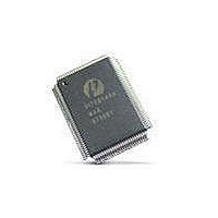
PI7C7300DNAE Pericom Semiconductor, PI7C7300DNAE Datasheet - Page 25

PI7C7300DNAE
Manufacturer Part Number
PI7C7300DNAE
Description
IC PCI-PCI BRIDGE 3PORT 272-BGA
Manufacturer
Pericom Semiconductor
Datasheet
1.PI7C7300DNAE.pdf
(107 pages)
Specifications of PI7C7300DNAE
Applications
*
Interface
*
Voltage - Supply
*
Package / Case
272-PBGA
Mounting Type
Surface Mount
Maximum Operating Temperature
+ 85 C
Minimum Operating Temperature
- 40 C
Mounting Style
SMD/SMT
Operating Supply Voltage
3 V to 3.6 V
Supply Current (max)
660 mA
Lead Free Status / RoHS Status
Lead free / RoHS Compliant
Available stocks
Company
Part Number
Manufacturer
Quantity
Price
Company:
Part Number:
PI7C7300DNAE
Manufacturer:
Pericom
Quantity:
135
Company:
Part Number:
PI7C7300DNAE
Manufacturer:
MAX
Quantity:
5 510
4.6.2
4.6.3
Pericom Semiconductor
MEMORY WRITE AND INVALIDATE TRANSACTIONS
Posted write forwarding is used for Memory Write and Invalidate transactions.
The PI7C7300D disconnects Memory Write and Invalidate commands at aligned cache
line boundaries. The cache line size value in the cache line size register gives the number
of DWORD in a cache line.
If the value in the cache line size register does meet the memory write and invalidate
conditions, the PI7C7300D returns a target disconnect to the initiator either on a cache
line boundary or when the posted write buffer fills.
When the Memory Write and Invalidate transaction is disconnected before a cache line
boundary is reached, typically because the posted write buffer fills, the trans-action is
converted to Memory Write transaction.
DELAYED WRITE TRANSACTIONS
Delayed write forwarding is used for I/O write transactions and Type 1 configuration
write transactions.
A delayed write transaction guarantees that the actual target response is returned back to
the initiator without holding the initiating bus in wait states. A delayed write transaction
is limited to a single DWORD data transfer.
When a write transaction is first detected on the initiator bus, and PI7C7300D forwards it
as a delayed transaction, PI7C7300D claims the access by asserting DEVSEL# and
returns a target retry to the initiator. During the address phase, PI7C7300D samples the
bus command, address, and address parity one cycle later. After IRDY# is asserted,
PI7C7300D also samples the first data DWORD, byte enable bits, and data parity. This
information is placed into the delayed transaction queue. The transaction is queued only
if no other existing delayed transactions have the same address and command, and if the
delayed transaction queue is not full. When the delayed write transaction moves to the
head of the delayed transaction queue and all ordering constraints with posted data are
satisfied. The PI7C7300D initiates the transaction on the target bus. PI7C7300D
transfers the write data to the target. If PI7C7300D receives a target retry
in response to the write transaction on the target bus, it continues to repeat the write
transaction until the data transfer is completed, or until an error condition is encountered.
If PI7C7300D is unable to deliver write data after 2
attempts, PI7C7300D will report a system error. PI7C7300D also asserts P_SERR# if the
primary SERR# enable bit is set in the command register. See Section 7.4 for information
on the assertion of P_SERR#. When the initiator repeats the same write transaction (same
command, address, byte enable bits, and data), and the completed delayed transaction is
at the head of the queue, the PI7C7300D claims the access by asserting DEVSEL# and
returns TRDY# to the initiator, to indicate that the write data
was transferred. If the initiator requests multiple DWORD, PI7C7300D also asserts
STOP# in conjunction with TRDY# to signal a target disconnect. Note that only those
Page 25 of 107
24
(default) or 2
3-PORT PCI-TO-PCI BRIDGE
November 2005 - Revision 1.01
32
(maximum)
PI7C7300D


