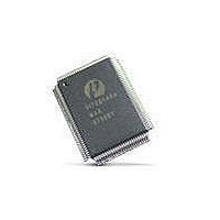
PI7C7300DNAE Pericom Semiconductor, PI7C7300DNAE Datasheet - Page 97

PI7C7300DNAE
Manufacturer Part Number
PI7C7300DNAE
Description
IC PCI-PCI BRIDGE 3PORT 272-BGA
Manufacturer
Pericom Semiconductor
Datasheet
1.PI7C7300DNAE.pdf
(107 pages)
Specifications of PI7C7300DNAE
Applications
*
Interface
*
Voltage - Supply
*
Package / Case
272-PBGA
Mounting Type
Surface Mount
Maximum Operating Temperature
+ 85 C
Minimum Operating Temperature
- 40 C
Mounting Style
SMD/SMT
Operating Supply Voltage
3 V to 3.6 V
Supply Current (max)
660 mA
Lead Free Status / RoHS Status
Lead free / RoHS Compliant
Available stocks
Company
Part Number
Manufacturer
Quantity
Price
Company:
Part Number:
PI7C7300DNAE
Manufacturer:
Pericom
Quantity:
135
Company:
Part Number:
PI7C7300DNAE
Manufacturer:
MAX
Quantity:
5 510
15.3.4
16
16.1
Pericom Semiconductor
SECONDARY IDSEL MAPPING
When PI7C7300D detects a Type 1 configuration transaction for a device connected to
the secondary, it translates the Type 1 transaction to Type 0 transaction on the
downstream interface. Type 1 configuration format uses a 5-bit field at P_AD[15:11] as a
device number. This is translated to S1_AD[31:16] or S2_AD[31:16] by PI7C7300D.
IEEE 1149.1 COMPATIBLE JTAG CONTROLLER
An IEEE 1149.1 compatible Test Access Port (TAP) controller and associated TAP pins
are provided to support boundary scan in PI7C7300D for board-level continuity test and
diagnostics. The TAP pins assigned are TCK, TDI, TDO, TMS and TRST#. All digital
input, output, input/output pins are tested except TAP pins and clock pin.
The IEEE 1149.1 Test Logic consists of a TAP controller, an instruction register, and
a group of test data registers including Bypass, Device Identification and Boundary Scan
registers. The TAP controller is a synchronous 16-state machine driven by the Test Clock
(TCK) and the Test Mode Select (TMS) pins. An independent power on reset circuit is
provided to ensure the machine is in TEST_LOGIC_RESET state at power-up. The
JTAG signal lines are not active when the PCI resource is operating PCI bus cycles.
PI7C7300D implements 3 basic instructions: BYPASS, SAMPLE/PRELOAD, and
EXTEST.
BOUNDARY SCAN ARCHITECTURE
Boundary-scan test logic consists of a boundary-scan register and support logic. These
are accessed through a Test Access Port (TAP). The TAP provides a simple serial
interface that allows all processor signal pins to be driven and/or sampled, thereby
providing direct control and monitoring of processor pins at the system level.
This mode of operation is valuable for design debugging and fault diagnosis since it
permits examination of connections not normally accessible to the test system. The
following subsections describe the boundary-scan test logic elements: TAP pins,
instruction register, test data registers and TAP controller. Error! Reference source not
found. illustrates how these pieces fit together to form the JTAG unit.
Page 97 of 107
3-PORT PCI-TO-PCI BRIDGE
November 2005 - Revision 1.01
PI7C7300D


