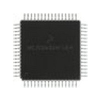
MC68HC705X32CFU Freescale Semiconductor, MC68HC705X32CFU Datasheet - Page 105

MC68HC705X32CFU
Manufacturer Part Number
MC68HC705X32CFU
Description
Manufacturer
Freescale Semiconductor
Datasheet
1.MC68HC705X32CFU.pdf
(232 pages)
Specifications of MC68HC705X32CFU
Cpu Family
HC05
Device Core Size
8b
Frequency (max)
4MHz
Interface Type
SCI
Program Memory Type
EPROM
Program Memory Size
32KB
Total Internal Ram Size
528Byte
# I/os (max)
32
Number Of Timers - General Purpose
1
Operating Supply Voltage (typ)
5V
Operating Supply Voltage (max)
5.5V
Operating Supply Voltage (min)
4.5V
On-chip Adc
8-chx8-bit
Instruction Set Architecture
CISC
Operating Temp Range
-40C to 85C
Operating Temperature Classification
Industrial
Mounting
Surface Mount
Pin Count
64
Package Type
PQFP
Lead Free Status / Rohs Status
Supplier Unconfirmed
Available stocks
Company
Part Number
Manufacturer
Quantity
Price
Part Number:
MC68HC705X32CFU4
Manufacturer:
FREESCALE
Quantity:
20 000
- Current page: 105 of 232
- Download datasheet (6Mb)
7.2
•
•
•
•
•
•
7.3
•
•
•
7.4
A block diagram of the SCI is shown in
select the ‘wake-up’ method (WAKE bit) and data word length (M bit) of the SCI. SCCR2 provides
control bits that individually enable the transmitter and receiver, enable system interrupts and
provide the wake-up enable bit (RWU) and the send break code bit (SBK). Control bits in the baud
rate register (BAUD) allow the user to select one of 32 different baud rates for the transmitter and
receiver (see
Data transmission is initiated by writing to the serial communications data register (SCDR).
Provided the transmitter is enabled, data stored in the SCDR is transferred to the transmit data
shift register. This transfer of data sets the transmit data register empty flag (TDRE) in the SCI
status register (SCSR) and generates an interrupt (if transmitter interrupts are enabled). The
transfer of data to the transmit data shift register is synchronized with the bit rate clock (see
the transmission complete flag (TC) in the SCSR is set (provided no pending data, preamble or
break is to be sent) and an interrupt is generated (if the transmit complete interrupt is enabled). If
the transmitter is disabled, and the data, preamble or break (in the transmit data shift register) has
been sent, the TC bit will also be set. This will also generate an interrupt if the transmission
complete interrupt enable bit (TCIE) is set. If the transmitter is disabled during a transmission, the
character being transmitted will be completed before the transmitter gives up control of the
TDO pin.
MC68HC05X16
Figure
Receiver wake-up function (idle line or address bit)
Idle line detection
Framing error detection
Noise detection
Overrun detection
Receiver data register full flag
Transmit data register empty flag
Transmit complete flag
Send break
7-2). All data is transmitted least significant bit first. Upon completion of data transmission,
Section
SCI receiver features
SCI transmitter features
Functional description
Freescale Semiconductor, Inc.
For More Information On This Product,
7.11.5).
SERIAL COMMUNICATIONS INTERFACE
Go to: www.freescale.com
Figure
7-1. Option bits in serial control register1 (SCCR1)
7-3
7
Related parts for MC68HC705X32CFU
Image
Part Number
Description
Manufacturer
Datasheet
Request
R
Part Number:
Description:
Manufacturer:
Freescale Semiconductor, Inc
Datasheet:
Part Number:
Description:
Manufacturer:
Freescale Semiconductor, Inc
Datasheet:
Part Number:
Description:
Manufacturer:
Freescale Semiconductor, Inc
Datasheet:
Part Number:
Description:
Manufacturer:
Freescale Semiconductor, Inc
Datasheet:
Part Number:
Description:
Manufacturer:
Freescale Semiconductor, Inc
Datasheet:
Part Number:
Description:
Manufacturer:
Freescale Semiconductor, Inc
Datasheet:
Part Number:
Description:
Manufacturer:
Freescale Semiconductor, Inc
Datasheet:
Part Number:
Description:
Manufacturer:
Freescale Semiconductor, Inc
Datasheet:
Part Number:
Description:
Manufacturer:
Freescale Semiconductor, Inc
Datasheet:
Part Number:
Description:
Manufacturer:
Freescale Semiconductor, Inc
Datasheet:
Part Number:
Description:
Manufacturer:
Freescale Semiconductor, Inc
Datasheet:
Part Number:
Description:
Manufacturer:
Freescale Semiconductor, Inc
Datasheet:
Part Number:
Description:
Manufacturer:
Freescale Semiconductor, Inc
Datasheet:
Part Number:
Description:
Manufacturer:
Freescale Semiconductor, Inc
Datasheet:
Part Number:
Description:
Manufacturer:
Freescale Semiconductor, Inc
Datasheet:


