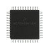
MC68HC705X32CFU Freescale Semiconductor, MC68HC705X32CFU Datasheet - Page 97

MC68HC705X32CFU
Manufacturer Part Number
MC68HC705X32CFU
Description
Manufacturer
Freescale Semiconductor
Datasheet
1.MC68HC705X32CFU.pdf
(232 pages)
Specifications of MC68HC705X32CFU
Cpu Family
HC05
Device Core Size
8b
Frequency (max)
4MHz
Interface Type
SCI
Program Memory Type
EPROM
Program Memory Size
32KB
Total Internal Ram Size
528Byte
# I/os (max)
32
Number Of Timers - General Purpose
1
Operating Supply Voltage (typ)
5V
Operating Supply Voltage (max)
5.5V
Operating Supply Voltage (min)
4.5V
On-chip Adc
8-chx8-bit
Instruction Set Architecture
CISC
Operating Temp Range
-40C to 85C
Operating Temperature Classification
Industrial
Mounting
Surface Mount
Pin Count
64
Package Type
PQFP
Lead Free Status / Rohs Status
Supplier Unconfirmed
Available stocks
Company
Part Number
Manufacturer
Quantity
Price
Part Number:
MC68HC705X32CFU4
Manufacturer:
FREESCALE
Quantity:
20 000
- Current page: 97 of 232
- Download datasheet (6Mb)
6.4
‘Output compare’ is a technique which may be used, for example, to generate an output waveform,
or to signal when a specific time period has elapsed, by presetting the output compare register to
the appropriate value.
There are two output compare registers: output compare register 1 (OCR1) and output compare
register 2 (OCR2).
Note:
6.4.1
The 16-bit output compare register 1 is made up of two 8-bit registers at locations $16 (MSB) and
$17 (LSB). The contents of the output compare register 1 are compared with the contents of the
free-running counter continually and, if a match is found, the corresponding output compare flag
(OCF1) in the timer status register is set and the output level (OLVL1) is transferred to pin TCMP1.
The output compare register 1 values and the output level bit should be changed after each
successful comparison to establish a new elapsed timeout. An interrupt can also accompany a
successful output compare provided the corresponding interrupt enable bit (OCIE) is set. (The
free-running counter is updated every four internal bus clock cycles.)
After a processor write cycle to the output compare register 1 containing the MSB ($16), the output
compare function is inhibited until the LSB ($17) is also written. The user must write both bytes
(locations) if the MSB is written first. A write made only to the LSB ($17) will not inhibit the compare
1 function. The processor can write to either byte of the output compare register 1 without affecting
the other byte. The output level (OLVL1) bit is clocked to the output level register and hence to the
TCMP1 pin whether the output compare flag 1 (OCF1) is set or clear. The minimum time required
to update the output compare register 1 is a function of the program rather than the internal
hardware. Because the output compare flag 1 and the output compare register 1 are not defined
at power on, and not affected by reset, care must be taken when initializing output compare
functions with software. The following procedure is recommended:
MC68HC05X16
Output compare high 1
Output compare low 1
– Write to output compare high 1 to inhibit further compares;
– Read the timer status register to clear OCF1 (if set);
– Write to output compare low 1 to enable the output compare 1 function.
The same output compare interrupt enable bit (OCIE) is used for the two output
compares.
Output compare
Output compare register 1 (OCR1)
Freescale Semiconductor, Inc.
For More Information On This Product,
Address
Go to: www.freescale.com
$0016
$0017
PROGRAMMABLE TIMER
bit 7
bit 6
bit 5
bit 4
bit 3
bit 2
bit 1
bit 0
Undefined
Undefined
on reset
State
6-9
6
Related parts for MC68HC705X32CFU
Image
Part Number
Description
Manufacturer
Datasheet
Request
R
Part Number:
Description:
Manufacturer:
Freescale Semiconductor, Inc
Datasheet:
Part Number:
Description:
Manufacturer:
Freescale Semiconductor, Inc
Datasheet:
Part Number:
Description:
Manufacturer:
Freescale Semiconductor, Inc
Datasheet:
Part Number:
Description:
Manufacturer:
Freescale Semiconductor, Inc
Datasheet:
Part Number:
Description:
Manufacturer:
Freescale Semiconductor, Inc
Datasheet:
Part Number:
Description:
Manufacturer:
Freescale Semiconductor, Inc
Datasheet:
Part Number:
Description:
Manufacturer:
Freescale Semiconductor, Inc
Datasheet:
Part Number:
Description:
Manufacturer:
Freescale Semiconductor, Inc
Datasheet:
Part Number:
Description:
Manufacturer:
Freescale Semiconductor, Inc
Datasheet:
Part Number:
Description:
Manufacturer:
Freescale Semiconductor, Inc
Datasheet:
Part Number:
Description:
Manufacturer:
Freescale Semiconductor, Inc
Datasheet:
Part Number:
Description:
Manufacturer:
Freescale Semiconductor, Inc
Datasheet:
Part Number:
Description:
Manufacturer:
Freescale Semiconductor, Inc
Datasheet:
Part Number:
Description:
Manufacturer:
Freescale Semiconductor, Inc
Datasheet:
Part Number:
Description:
Manufacturer:
Freescale Semiconductor, Inc
Datasheet:


