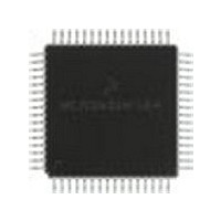
MC68HC705X32CFU Freescale Semiconductor, MC68HC705X32CFU Datasheet - Page 27

MC68HC705X32CFU
Manufacturer Part Number
MC68HC705X32CFU
Description
Manufacturer
Freescale Semiconductor
Datasheet
1.MC68HC705X32CFU.pdf
(232 pages)
Specifications of MC68HC705X32CFU
Cpu Family
HC05
Device Core Size
8b
Frequency (max)
4MHz
Interface Type
SCI
Program Memory Type
EPROM
Program Memory Size
32KB
Total Internal Ram Size
528Byte
# I/os (max)
32
Number Of Timers - General Purpose
1
Operating Supply Voltage (typ)
5V
Operating Supply Voltage (max)
5.5V
Operating Supply Voltage (min)
4.5V
On-chip Adc
8-chx8-bit
Instruction Set Architecture
CISC
Operating Temp Range
-40C to 85C
Operating Temperature Classification
Industrial
Mounting
Surface Mount
Pin Count
64
Package Type
PQFP
Lead Free Status / Rohs Status
Supplier Unconfirmed
Available stocks
Company
Part Number
Manufacturer
Quantity
Price
Part Number:
MC68HC705X32CFU4
Manufacturer:
FREESCALE
Quantity:
20 000
- Current page: 27 of 232
- Download datasheet (6Mb)
Note:
2.1.2.1
In the ‘load program in RAM and execute’ routine, user programs are loaded into MCU RAM via
the SCI port and then executed. Data is loaded sequentially, starting at RAM location $0050, until
the last byte is loaded. The first byte loaded is the count of the total number of bytes in the program
plus the count byte. After completion of RAM loading, control can be transferred either to the
second byte in RAM, $0051, by executing a jump to RAM + 1 function, or it can be transferred to
any address by executing a jump to any address function. During the firmware initialization stage,
the SCI is configured for the NRZ data format (idle line, start bit, eight data bits and stop bit). The
baud rate is 9600 with a 4 MHz crystal. A program to convert ASCII S-records to the format
required by the RAM loader is available from Motorola.
When the last byte is loaded, the firmware halts operation expecting additional data to arrive. At
this point, the reset switch is placed in the reset position which resets the MCU, but keeps the RAM
program intact. All routines loaded in RAM can now be entered from this state, including the one
which executes the program in RAM (see
To load a program in the EEPROM, the ‘load program in RAM and execute’ function is also used.
In this instance the process involves two distinct steps. Firstly, the RAM is loaded with a program
which controls the loading of the EEPROM, and when the RAM contents are executed, the MCU
is instructed to load the EEPROM.
The erased state of the EEPROM is $FF.
Figure 2-3
2.1.2.2
After the serial RAM loader program is completed this function can be used to execute a program
loaded in RAM starting at the second RAM address, $0051. It must be noted that the lowest RAM
address, $0050, is used by the RAM loader program to store the total number of bytes in the
program.
2.1.2.3
This function allows execution of programs previously loaded in RAM or EEPROM using the
methods outlined in
To execute the ‘jump to any address’ function, data input at port A has to be $CC and data input at
port B and port C should represent the MSB and LSB respectively, of the address to jump to for
execution of the user program. A schematic diagram of the circuit required is shown in
MC68HC05X16
Oscillator divide-by-two is forced in bootstrap mode; all other mask options are selected
by the customer (see
shows the schematic diagram of the circuit required for the serial RAM loader.
Serial RAM loader
Jump to RAM + 1
‘Jump to any address’
Freescale Semiconductor, Inc.
Section
For More Information On This Product,
MODES OF OPERATION AND PIN DESCRIPTIONS
2.1.2.1.
Go to: www.freescale.com
Section
1.2).
Section 2.1.2.2
and
Section
2.1.2.3).
Figure
2-2.
2-3
2
Related parts for MC68HC705X32CFU
Image
Part Number
Description
Manufacturer
Datasheet
Request
R
Part Number:
Description:
Manufacturer:
Freescale Semiconductor, Inc
Datasheet:
Part Number:
Description:
Manufacturer:
Freescale Semiconductor, Inc
Datasheet:
Part Number:
Description:
Manufacturer:
Freescale Semiconductor, Inc
Datasheet:
Part Number:
Description:
Manufacturer:
Freescale Semiconductor, Inc
Datasheet:
Part Number:
Description:
Manufacturer:
Freescale Semiconductor, Inc
Datasheet:
Part Number:
Description:
Manufacturer:
Freescale Semiconductor, Inc
Datasheet:
Part Number:
Description:
Manufacturer:
Freescale Semiconductor, Inc
Datasheet:
Part Number:
Description:
Manufacturer:
Freescale Semiconductor, Inc
Datasheet:
Part Number:
Description:
Manufacturer:
Freescale Semiconductor, Inc
Datasheet:
Part Number:
Description:
Manufacturer:
Freescale Semiconductor, Inc
Datasheet:
Part Number:
Description:
Manufacturer:
Freescale Semiconductor, Inc
Datasheet:
Part Number:
Description:
Manufacturer:
Freescale Semiconductor, Inc
Datasheet:
Part Number:
Description:
Manufacturer:
Freescale Semiconductor, Inc
Datasheet:
Part Number:
Description:
Manufacturer:
Freescale Semiconductor, Inc
Datasheet:
Part Number:
Description:
Manufacturer:
Freescale Semiconductor, Inc
Datasheet:


