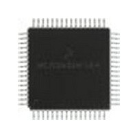
MC68HC705X32CFU Freescale Semiconductor, MC68HC705X32CFU Datasheet - Page 129

MC68HC705X32CFU
Manufacturer Part Number
MC68HC705X32CFU
Description
Manufacturer
Freescale Semiconductor
Datasheet
1.MC68HC705X32CFU.pdf
(232 pages)
Specifications of MC68HC705X32CFU
Cpu Family
HC05
Device Core Size
8b
Frequency (max)
4MHz
Interface Type
SCI
Program Memory Type
EPROM
Program Memory Size
32KB
Total Internal Ram Size
528Byte
# I/os (max)
32
Number Of Timers - General Purpose
1
Operating Supply Voltage (typ)
5V
Operating Supply Voltage (max)
5.5V
Operating Supply Voltage (min)
4.5V
On-chip Adc
8-chx8-bit
Instruction Set Architecture
CISC
Operating Temp Range
-40C to 85C
Operating Temperature Classification
Industrial
Mounting
Surface Mount
Pin Count
64
Package Type
PQFP
Lead Free Status / Rohs Status
Supplier Unconfirmed
Available stocks
Company
Part Number
Manufacturer
Quantity
Price
Part Number:
MC68HC705X32CFU4
Manufacturer:
FREESCALE
Quantity:
20 000
- Current page: 129 of 232
- Download datasheet (6Mb)
Freescale Semiconductor, Inc.
9
ANALOG TO DIGITAL CONVERTER
The analog to digital converter system consists of a single 8-bit successive approximation
converter and a sixteen channel multiplexer. Eight of the channels are connected to the
PD0/AN0 – PD7/AN7 pins of the MC68HC05X16 and the other eight channels are dedicated to
internal reference points for test functions. The channel input pins do not have any internal output
driver circuitry connected to them because such circuitry would load the analog input signals due
to output buffer leakage current. There is one 8-bit result data register (address $08) and one 8-bit
status/control register (address $09).
The A/D converter is ratiometric and two dedicated pins, VRH and VRL, are used to supply the
reference voltage levels for all analog inputs. These pins are used in preference to the system
power supply lines because any voltage drops in the bonding wires of the heavily loaded supply
pins could degrade the accuracy of the A/D conversion. An input voltage equal to or greater than
V
converts to $FF (full scale) with no overflow indication and an input voltage equal to V
RH
RL
converts to $00.
The A/D converter can operate from either the bus clock or an internal RC type oscillator. The
9
internal RC type oscillator is activated by the ADRC bit in the A/D status/control register (ADSTAT)
and can be used to give a sufficiently high clock rate to the A/D converter when the bus speed is too
low to provide accurate results. When the A/D converter is not being used it can be disconnected,
by clearing the ADON bit in the ADSTAT register, in order to save power (see
Section
9.2.3).
For further information on A/D converter operation please refer to the M68HC11 Reference
Manual — M68HC11RM/AD.
9.1
A/D converter operation
The A/D converter consists of an analog multiplexer, an 8-bit digital to analog converter capacitor
array, a comparator and a successive approximation register (SAR) (see
Figure
9-1).
There are eleven options that can be selected by the multiplexer; AN0–AN7, VRH, (VRH+VRL)/2
or VRL. Selection is done via the CHx bits in the ADSTAT register (see
Section
9.2.3). AN0–AN7
are the only input points for A/D conversion operations; the others are reference points that can be
used for test purposes.
MC68HC05X16
ANALOG TO DIGITAL CONVERTER
For More Information On This Product,
9-1
Go to: www.freescale.com
Related parts for MC68HC705X32CFU
Image
Part Number
Description
Manufacturer
Datasheet
Request
R
Part Number:
Description:
Manufacturer:
Freescale Semiconductor, Inc
Datasheet:
Part Number:
Description:
Manufacturer:
Freescale Semiconductor, Inc
Datasheet:
Part Number:
Description:
Manufacturer:
Freescale Semiconductor, Inc
Datasheet:
Part Number:
Description:
Manufacturer:
Freescale Semiconductor, Inc
Datasheet:
Part Number:
Description:
Manufacturer:
Freescale Semiconductor, Inc
Datasheet:
Part Number:
Description:
Manufacturer:
Freescale Semiconductor, Inc
Datasheet:
Part Number:
Description:
Manufacturer:
Freescale Semiconductor, Inc
Datasheet:
Part Number:
Description:
Manufacturer:
Freescale Semiconductor, Inc
Datasheet:
Part Number:
Description:
Manufacturer:
Freescale Semiconductor, Inc
Datasheet:
Part Number:
Description:
Manufacturer:
Freescale Semiconductor, Inc
Datasheet:
Part Number:
Description:
Manufacturer:
Freescale Semiconductor, Inc
Datasheet:
Part Number:
Description:
Manufacturer:
Freescale Semiconductor, Inc
Datasheet:
Part Number:
Description:
Manufacturer:
Freescale Semiconductor, Inc
Datasheet:
Part Number:
Description:
Manufacturer:
Freescale Semiconductor, Inc
Datasheet:
Part Number:
Description:
Manufacturer:
Freescale Semiconductor, Inc
Datasheet:


