PCM18XK1 Microchip Technology, PCM18XK1 Datasheet - Page 148
PCM18XK1
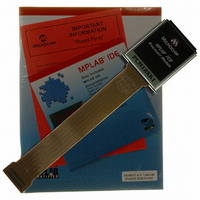
Manufacturer Part Number
PCM18XK1
Description
MODULE PROC PIC18F8680,6680,8565
Manufacturer
Microchip Technology
Datasheet
1.PCM18XK1.pdf
(496 pages)
Specifications of PCM18XK1
Accessory Type
Processor Module
Lead Free Status / RoHS Status
Not applicable / Not applicable
For Use With/related Products
ICE2000
For Use With
ICE2000 - EMULATOR MPLAB-ICE 2000 POD
Lead Free Status / Rohs Status
Lead free / RoHS Compliant


PIC18F6585/8585/6680/8680
10.8
PORTH is an 8-bit wide, bidirectional I/O port. The cor-
responding data direction register is TRISH. Setting a
TRISH bit (= 1) will make the corresponding PORTH
pin an input (i.e., put the corresponding output driver in
a high-impedance mode). Clearing a TRISH bit (= 0)
will make the corresponding PORTH pin an output (i.e.,
put the contents of the output latch on the selected pin).
Read-modify-write operations on the LATH register
read and write the latched output value for PORTH.
Pins RH7:RH4 are multiplexed with analog inputs
AN15:AN12. Pins RH3:RH0 are multiplexed with the
system bus as the external memory interface; they are
the high-order address bits, A19:A16. By default, pins
RH7:RH4 are enabled as A/D inputs and pins
RH3:RH0 are enabled as the system address bus.
Register ADCON1 configures RH7:RH4 as I/O or A/D
inputs. Register MEMCON configures RH3:RH0 as I/O
or system bus pins.
Pins RH7 and RH6 can be configured as the alternate
peripheral pins for CCP1 PWM output P1B and P1C,
respectively. This is done by clearing the configuration
bit ECCPMX, in configuration register CONFIG3H
(CONFIG3H<1>).
EXAMPLE 10-8:
DS30491C-page 146
CLRF
CLRF
MOVLW
MOVWF
MOVLW
MOVWF
Note:
Note 1: On
2: On
PORTH, LATH and TRISH
Registers
PORTH
LATH
0Fh
ADCON1
0CFh
TRISH
PORTH is available only on PIC18F8X8X
devices.
RH7:RH4 default to A/D inputs and read
as ‘0’.
RH3:RH0 default to system bus signals.
Power-on
Power-on
INITIALIZING PORTH
; Initialize PORTH by
; clearing output
; data latches
; Alternate method
; to clear output
; data latches
;
;
; Value used to
; initialize data
; direction
; Set RH3:RH0 as inputs
; RH5:RH4 as outputs
; RH7:RH6 as inputs
Reset,
Reset,
PORTH
PORTH
pins
pins
FIGURE 10-22:
FIGURE 10-23:
Note 1: I/O pins have diode protection to V
RD LATH
WR LATH
or
PORTH
RD TRISH
RD PORTH
Note 1: I/O pins have diode protection to V
RD LATH
Data
Bus
Data
Bus
WR TRISH
WR LATH
or
PORTH
RD TRISH
RD PORTH
WR TRISH
To A/D Converter
TRIS Latch
Data Latch
TRIS Latch
Data Latch
D
D
D
D
CK
CK
CK
CK
RH3:RH0 PINS BLOCK
DIAGRAM IN I/O MODE
Q
RH7:RH4 PINS BLOCK
DIAGRAM IN I/O MODE
Q
Q
2004 Microchip Technology Inc.
Q
Q
Q
EN
EN
Schmitt
Trigger
Input
Buffer
EN
Schmitt
Trigger
Input
Buffer
EN
D
D
DD
DD
and V
and V
I/O pin
I/O pin
SS
SS
(1)
.
.
(1)
Related parts for PCM18XK1
Image
Part Number
Description
Manufacturer
Datasheet
Request
R

Part Number:
Description:
Manufacturer:
Microchip Technology Inc.
Datasheet:
Part Number:
Description:
Manufacturer:
Microchip Technology Inc.
Datasheet:
Part Number:
Description:
Manufacturer:
Microchip Technology Inc.
Datasheet:
Part Number:
Description:
Manufacturer:
Microchip Technology Inc.
Datasheet:
Part Number:
Description:
Manufacturer:
Microchip Technology Inc.
Datasheet:
Part Number:
Description:
Manufacturer:
Microchip Technology Inc.
Datasheet:
Part Number:
Description:
Manufacturer:
Microchip Technology Inc.
Datasheet:
Part Number:
Description:
Manufacturer:
Microchip Technology Inc.
Datasheet: