PCM18XK1 Microchip Technology, PCM18XK1 Datasheet - Page 404
PCM18XK1
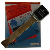
Manufacturer Part Number
PCM18XK1
Description
MODULE PROC PIC18F8680,6680,8565
Manufacturer
Microchip Technology
Datasheet
1.PCM18XK1.pdf
(496 pages)
Specifications of PCM18XK1
Accessory Type
Processor Module
Lead Free Status / RoHS Status
Not applicable / Not applicable
For Use With/related Products
ICE2000
For Use With
ICE2000 - EMULATOR MPLAB-ICE 2000 POD
Lead Free Status / Rohs Status
Lead free / RoHS Compliant


PIC18F6585/8585/6680/8680
SUBWFB
Syntax:
Operands:
Operation:
Status Affected:
Encoding:
Description:
Words:
Cycles:
Example 1:
Example 2:
Example 3:
DS30491C-page 402
Q Cycle Activity:
Before Instruction
After Instruction
Before Instruction
After Instruction
Before Instruction
After Instruction
Decode
REG
W
C
REG
W
C
Z
N
REG
W
C
REG
W
C
Z
N
REG
W
C
REG
W
C
Z
N
Q1
=
=
=
=
=
=
=
=
=
=
=
=
=
=
=
=
=
=
=
=
=
=
=
=
register ‘f’
Subtract W from f with Borrow
[ label ] SUBWFB
0
d
a
(f) – (W) – (C)
N, OV, C, DC, Z
Subtract W and the Carry flag (bor-
row) from register ‘f’ (2’s complement
method). If ‘d’ is ‘0’, the result is
stored in W. If ‘d’ is ‘1’, the result is
stored back in register ‘f’ (default). If
‘a’ is ‘0’, the Access Bank will be
selected, overriding the BSR value. If
‘a’ is ‘1’, then the bank will be
selected as per the BSR value
(default).
1
1
SUBWFB
SUBWFB REG, 0, 0
SUBWFB
Read
0101
Q2
f
0x19
0x0D
1
0x0C
0x0D
1
0
0
0x1B
0x1A
0
0x1B
0x00
1
1
0
0x03
0x0E
1
0xF5
0x0E
0
0
1
[0,1]
[0,1]
255
10da
REG, 1, 0
REG, 1, 0
(0001 1001)
(0000 1101)
(0000 1011)
(0000 1101)
; result is positive
(0001 1011)
(0001 1010)
(0001 1011)
; result is zero
(0000 0011)
(0000 1101)
(1111 0100)
; [2’s comp]
(0000 1101)
; result is negative
Process
Data
Q3
dest
ffff
f [,d [,a]]
destination
Write to
Q4
ffff
SWAPF
Syntax:
Operands:
Operation:
Status Affected:
Encoding:
Description:
Words:
Cycles:
Example:
Q Cycle Activity:
Before Instruction
After Instruction
Decode
REG
REG
Q1
=
=
register ‘f’
Swap f
[ label ] SWAPF f [,d [,a]]
0
d
a
(f<3:0>)
(f<7:4>)
None
The upper and lower nibbles of
register ‘f’ are exchanged. If ‘d’ is
‘0’, the result is placed in W. If ‘d’ is
‘1’, the result is placed in register ‘f’
(default). If ‘a’ is ‘0’, the Access
Bank will be selected, overriding
the BSR value. If ‘a’ is ‘1’, then the
bank will be selected as per the
BSR value (default).
1
1
SWAPF
Read
0011
Q2
0x53
0x35
f
[0,1]
[0,1]
2004 Microchip Technology Inc.
255
REG, 1, 0
10da
dest<7:4>,
dest<3:0>
Process
Data
Q3
ffff
destination
Write to
Q4
ffff
Related parts for PCM18XK1
Image
Part Number
Description
Manufacturer
Datasheet
Request
R

Part Number:
Description:
Manufacturer:
Microchip Technology Inc.
Datasheet:
Part Number:
Description:
Manufacturer:
Microchip Technology Inc.
Datasheet:
Part Number:
Description:
Manufacturer:
Microchip Technology Inc.
Datasheet:
Part Number:
Description:
Manufacturer:
Microchip Technology Inc.
Datasheet:
Part Number:
Description:
Manufacturer:
Microchip Technology Inc.
Datasheet:
Part Number:
Description:
Manufacturer:
Microchip Technology Inc.
Datasheet:
Part Number:
Description:
Manufacturer:
Microchip Technology Inc.
Datasheet:
Part Number:
Description:
Manufacturer:
Microchip Technology Inc.
Datasheet: