PCM18XK1 Microchip Technology, PCM18XK1 Datasheet - Page 94
PCM18XK1
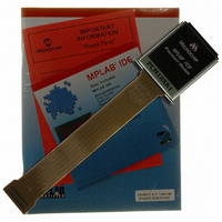
Manufacturer Part Number
PCM18XK1
Description
MODULE PROC PIC18F8680,6680,8565
Manufacturer
Microchip Technology
Datasheet
1.PCM18XK1.pdf
(496 pages)
Specifications of PCM18XK1
Accessory Type
Processor Module
Lead Free Status / RoHS Status
Not applicable / Not applicable
For Use With/related Products
ICE2000
For Use With
ICE2000 - EMULATOR MPLAB-ICE 2000 POD
Lead Free Status / Rohs Status
Lead free / RoHS Compliant


PIC18F6585/8585/6680/8680
5.5.2
Depending on the application, good programming
practice may dictate that the value written to the mem-
ory should be verified against the original value. This
should be used in applications where excessive writes
can stress bits near the specification limit.
5.5.3
If a write is terminated by an unplanned event, such as
loss of power or an unexpected Reset, the memory
location just programmed should be verified and repro-
grammed if needed. The WRERR bit is set when a
write operation is interrupted by a MCLR Reset or a
WDT Time-out Reset during normal operation. In these
situations, users can check the WRERR bit and rewrite
the location.
TABLE 5-2:
DS30491C-page 92
TBLPTRU
TBPLTRH
TBLPTRL
TABLAT
INTCON
EECON2
EECON1
IPR2
PIR2
PIE2
Legend:
Name
x = unknown, u = unchanged, r = reserved, – = unimplemented, read as ‘0’.
Shaded cells are not used during Flash/EEPROM access.
WRITE VERIFY
UNEXPECTED TERMINATION OF
WRITE OPERATION
Program Memory Table Pointer High Byte (TBLPTR<15:8>)
Program Memory Table Pointer High Byte (TBLPTR<7:0>)
Program Memory Table Latch
EEPROM Control Register 2 (not a physical register)
GIE/GIEH PEIE/GIEL TMR0IE
EEPGD
Bit 7
—
—
—
—
REGISTERS ASSOCIATED WITH PROGRAM FLASH MEMORY
CFGS
CMIP
CMIE
CMIF
Bit 6
—
bit 21
Bit 5
—
—
—
—
Program Memory Table Pointer Upper Byte
(TBLPTR<20:16>)
FREE
INTE
EEIP
EEIF
EEIE
Bit 4
WRERR
BCLIP
BCLIF
BCLIE
RBIE
Bit 3
TMR0IF
WREN
LVDIP
LVDIE
LVDIF
5.5.4
To protect against spurious writes to Flash program
memory, the write initiate sequence must also be
followed. See Section 24.0 “Special Features of the
CPU” for more detail.
5.6
See Section 24.0 “Special Features of the CPU” for
details on code protection of Flash program memory.
Bit 2
TMR3IP
TMR3IF
TMR3IE
Flash Program Operation During
Code Protection
INTF
Bit 1
WR
PROTECTION AGAINST SPURIOUS
WRITES
CCP2IP
CCP2IF
CCP2IE
RBIF
Bit 0
RD
2004 Microchip Technology Inc.
--00 0000
0000 0000
0000 0000
0000 0000
0000 0000
xx-0 x000
-1-1 1111
-0-0 0000
-0-0 0000
POR, BOR
Value on:
—
--00 0000
0000 0000
0000 0000
0000 0000
0000 0000
uu-0 u000
-1-1 1111
-0-0 0000
-0-0 0000
Value on
all other
Resets
—
Related parts for PCM18XK1
Image
Part Number
Description
Manufacturer
Datasheet
Request
R

Part Number:
Description:
Manufacturer:
Microchip Technology Inc.
Datasheet:
Part Number:
Description:
Manufacturer:
Microchip Technology Inc.
Datasheet:
Part Number:
Description:
Manufacturer:
Microchip Technology Inc.
Datasheet:
Part Number:
Description:
Manufacturer:
Microchip Technology Inc.
Datasheet:
Part Number:
Description:
Manufacturer:
Microchip Technology Inc.
Datasheet:
Part Number:
Description:
Manufacturer:
Microchip Technology Inc.
Datasheet:
Part Number:
Description:
Manufacturer:
Microchip Technology Inc.
Datasheet:
Part Number:
Description:
Manufacturer:
Microchip Technology Inc.
Datasheet: