PCM18XK1 Microchip Technology, PCM18XK1 Datasheet - Page 59
PCM18XK1
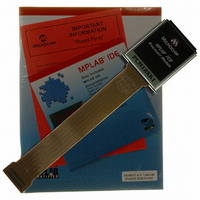
Manufacturer Part Number
PCM18XK1
Description
MODULE PROC PIC18F8680,6680,8565
Manufacturer
Microchip Technology
Datasheet
1.PCM18XK1.pdf
(496 pages)
Specifications of PCM18XK1
Accessory Type
Processor Module
Lead Free Status / RoHS Status
Not applicable / Not applicable
For Use With/related Products
ICE2000
For Use With
ICE2000 - EMULATOR MPLAB-ICE 2000 POD
Lead Free Status / Rohs Status
Lead free / RoHS Compliant


4.6
An “Instruction Cycle” consists of four Q cycles (Q1,
Q2, Q3 and Q4). The instruction fetch and execute are
pipelined such that fetch takes one instruction cycle,
while decode and execute takes another instruction
cycle. However, due to the pipelining each instruction
effectively executes in one cycle. If an instruction
causes the program counter to change (e.g., GOTO),
then two cycles are required to complete the instruction
(Example 4-2).
EXAMPLE 4-2:
4.7
The program memory is addressed in bytes. Instruc-
tions are stored as two bytes or four bytes in program
memory. The Least Significant Byte (LSB) of an
instruction word is always stored in a program memory
location with an even address (LSB = 0). Figure 4-6
shows an example of how instruction words are stored
in the program memory. To maintain alignment with
instruction boundaries, the PC increments in steps of 2
and the LSB will always read ‘0’ (see Section 4.4
“PCL, PCLATH and PCLATU”).
FIGURE 4-6:
2004 Microchip Technology Inc.
1. MOVLW 55h
2. MOVWF PORTB
3. BRA
4. BSF
5. Instruction @ address SUB_1
All instructions are single cycle except for any program branches. These take two cycles since the fetch instruction
is “flushed” from the pipeline while the new instruction is being fetched and then executed.
Instruction Flow/Pipelining
Instructions in Program Memory
SUB_1
PORTA, 3 (Forced NOP)
Instruction 1:
Instruction 2:
Instruction 3:
INSTRUCTION PIPELINE FLOW
INSTRUCTIONS IN PROGRAM MEMORY
Program Memory
Byte Locations
MOVLW
GOTO
MOVFF
Fetch 1
T
CY
0
055h
000006h
123h, 456h
Execute 1
Fetch 2
PIC18F6585/8585/6680/8680
T
CY
1
Execute 2
Fetch 3
LSB = 1
T
0EFh
0F0h
0C1h
0F4h
CY
0Fh
2
A fetch cycle begins with the program counter (PC)
incrementing in Q1.
In the execution cycle, the fetched instruction is latched
into the “Instruction Register” (IR) in cycle Q1. This
instruction is then decoded and executed during the
Q2, Q3, and Q4 cycles. Data memory is read during Q2
(operand read) and written during Q4 (destination
write).
The CALL and GOTO instructions have an absolute pro-
gram memory address embedded into the instruction.
Since instructions are always stored on word bound-
aries, the data contained in the instruction is a word
address. The word address is written to PC<20:1>
which accesses the desired byte address in program
memory. Instruction #2 in Figure 4-6 shows how the
instruction “GOTO 000006h” is encoded in the program
memory. Program branch instructions which encode a
relative address offset operate in the same manner.
The offset value stored in a branch instruction repre-
sents the number of single-word instructions that the
PC will be offset by. Section 25.0 “Instruction Set
Summary” provides further details of the instruction
set.
Execute 3
Fetch 4
LSB = 0
T
CY
55h
03h
00h
23h
56h
3
Fetch SUB_1 Execute SUB_1
Flush (NOP)
Word Address
000000h
000002h
000004h
000006h
000008h
00000Ah
00000Ch
00000Eh
000010h
000012h
000014h
T
CY
4
DS30491C-page 57
T
CY
5
Related parts for PCM18XK1
Image
Part Number
Description
Manufacturer
Datasheet
Request
R

Part Number:
Description:
Manufacturer:
Microchip Technology Inc.
Datasheet:
Part Number:
Description:
Manufacturer:
Microchip Technology Inc.
Datasheet:
Part Number:
Description:
Manufacturer:
Microchip Technology Inc.
Datasheet:
Part Number:
Description:
Manufacturer:
Microchip Technology Inc.
Datasheet:
Part Number:
Description:
Manufacturer:
Microchip Technology Inc.
Datasheet:
Part Number:
Description:
Manufacturer:
Microchip Technology Inc.
Datasheet:
Part Number:
Description:
Manufacturer:
Microchip Technology Inc.
Datasheet:
Part Number:
Description:
Manufacturer:
Microchip Technology Inc.
Datasheet: