PCM18XK1 Microchip Technology, PCM18XK1 Datasheet - Page 85
PCM18XK1
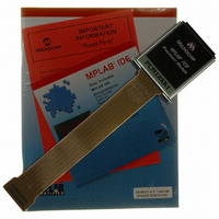
Manufacturer Part Number
PCM18XK1
Description
MODULE PROC PIC18F8680,6680,8565
Manufacturer
Microchip Technology
Datasheet
1.PCM18XK1.pdf
(496 pages)
Specifications of PCM18XK1
Accessory Type
Processor Module
Lead Free Status / RoHS Status
Not applicable / Not applicable
For Use With/related Products
ICE2000
For Use With
ICE2000 - EMULATOR MPLAB-ICE 2000 POD
Lead Free Status / Rohs Status
Lead free / RoHS Compliant


5.0
The Flash program memory is readable, writable and
erasable during normal operation over the entire V
range.
A read from program memory is executed on one byte
at a time. A write to program memory is executed on
blocks of 8 bytes at a time. Program memory is erased
in blocks of 64 bytes at a time. A bulk erase operation
cannot be issued from user code.
Writing or erasing program memory will cease
instruction fetches until the operation is complete. The
program memory cannot be accessed during the write
or erase, therefore, code cannot execute. An internal
programming timer terminates program memory writes
and erases.
A value written to program memory does not need to be
a valid instruction. Executing a program memory
location that forms an invalid instruction results in a
NOP.
FIGURE 5-1:
2004 Microchip Technology Inc.
Note 1: Table Pointer points to a byte in program memory.
TBLPTRU
FLASH PROGRAM MEMORY
Table Pointer
TBLPTRH
TABLE READ OPERATION
(1)
TBLPTRL
Program Memory
(TBLPTR)
PIC18F6585/8585/6680/8680
DD
Instruction: TBLRD*
Program Memory
5.1
In order to read and write program memory, there are
two operations that allow the processor to move bytes
between the program memory space and the data RAM:
• Table Read (TBLRD)
• Table Write (TBLWT)
The program memory space is 16 bits wide, while the
data RAM space is 8-bits wide. Table reads and table
writes move data between these two memory spaces
through an 8-bit register (TABLAT).
Table read operations retrieve data from program
memory and places it into the data RAM space.
Figure 5-1 shows the operation of a table read with
program memory and data RAM.
Table write operations store data from the data memory
space into holding registers in program memory. The
procedure to write the contents of the holding
registers into
Section 5.5 “Writing to Flash Program Memory”.
Figure 5-2 shows the operation of a table write with
program memory and data RAM.
Table operations work with byte entities. A table block
containing data, rather than program instructions, is not
required to be word aligned. Therefore, a table block can
start and end at any byte address. If a table write is being
used to write executable code into program memory,
program instructions will need to be word aligned.
Table Reads and Table Writes
program
memory
Table Latch (8-bit)
TABLAT
DS30491C-page 83
is
detailed
in
Related parts for PCM18XK1
Image
Part Number
Description
Manufacturer
Datasheet
Request
R

Part Number:
Description:
Manufacturer:
Microchip Technology Inc.
Datasheet:
Part Number:
Description:
Manufacturer:
Microchip Technology Inc.
Datasheet:
Part Number:
Description:
Manufacturer:
Microchip Technology Inc.
Datasheet:
Part Number:
Description:
Manufacturer:
Microchip Technology Inc.
Datasheet:
Part Number:
Description:
Manufacturer:
Microchip Technology Inc.
Datasheet:
Part Number:
Description:
Manufacturer:
Microchip Technology Inc.
Datasheet:
Part Number:
Description:
Manufacturer:
Microchip Technology Inc.
Datasheet:
Part Number:
Description:
Manufacturer:
Microchip Technology Inc.
Datasheet: