PCM18XK1 Microchip Technology, PCM18XK1 Datasheet - Page 204
PCM18XK1
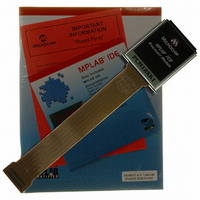
Manufacturer Part Number
PCM18XK1
Description
MODULE PROC PIC18F8680,6680,8565
Manufacturer
Microchip Technology
Datasheet
1.PCM18XK1.pdf
(496 pages)
Specifications of PCM18XK1
Accessory Type
Processor Module
Lead Free Status / RoHS Status
Not applicable / Not applicable
For Use With/related Products
ICE2000
For Use With
ICE2000 - EMULATOR MPLAB-ICE 2000 POD
Lead Free Status / Rohs Status
Lead free / RoHS Compliant


PIC18F6585/8585/6680/8680
17.4.2
The MSSP module functions are enabled by setting
MSSP Enable bit, SSPEN (SSPCON<5>).
The SSPCON1 register allows control of the I
ation. Four mode selection bits (SSPCON<3:0>) allow
one of the following I
• I
• I
• I
• I
• I
• I
Selection of any I
forces the SCL and SDA pins to be open-drain, pro-
vided these pins are programmed to inputs by setting
the appropriate TRISC bits. To ensure proper operation
of the module, pull-up resistors must be provided
externally to the SCL and SDA pins.
17.4.3
In Slave mode, the SCL and SDA pins must be config-
ured as inputs (TRISC<4:3> set). The MSSP module
will override the input state with the output data when
required (slave-transmitter).
The I
interrupt on an address match. Through the mode
select bits, the user can also choose to interrupt on
Start and Stop bits
When an address is matched or the data transfer after
an address match is received, the hardware automati-
cally will generate the Acknowledge (ACK) pulse and
load the SSPBUF register with the received value
currently in the SSPSR register.
Any combination of the following conditions will cause
the MSSP module not to give this ACK pulse:
• The buffer full bit BF (SSPSTAT<0>) was set
• The overflow bit SSPOV (SSPCON<6>) was set
In this case, the SSPSR register value is not loaded
into the SSPBUF but bit SSPIF (PIR1<3>) is set. The
BF bit is cleared by reading the SSPBUF register while
bit SSPOV is cleared through software.
The SCL clock input must have a minimum high and
low for proper operation. The high and low times of the
I
MSSP module, are shown in timing parameter #100
and parameter #101.
DS30491C-page 202
2
C specification, as well as the requirement of the
Stop bit interrupts enabled
Stop bit interrupts enabled
Idle
before the transfer was received.
before the transfer was received.
2
2
2
2
2
2
C Master mode, clock = OSC/4 (SSPADD + 1)
C Slave mode (7-bit address)
C Slave mode (10-bit address)
C Slave mode (7-bit address) with Start and
C Slave mode (10-bit address) with Start and
C Firmware Controlled Master mode, slave is
2
C Slave mode hardware will always generate an
OPERATION
SLAVE MODE
2
C mode with the SSPEN bit set,
2
C modes to be selected:
2
C oper-
17.4.3.1
Once the MSSP module has been enabled, it waits for
a Start condition to occur. Following the Start condition,
the 8 bits are shifted into the SSPSR register. All incom-
ing bits are sampled with the rising edge of the clock
(SCL) line. The value of register SSPSR<7:1> is com-
pared to the value of the SSPADD register. The
address is compared on the falling edge of the eighth
clock (SCL) pulse. If the addresses match and the BF
and SSPOV bits are clear, the following events occur:
1.
2.
3.
4.
In 10-bit Address mode, two address bytes need to be
received by the slave. The five Most Significant bits
(MSbs) of the first address byte specify if this is a 10-bit
address. Bit R/W (SSPSTAT<2>) must specify a write
so the slave device will receive the second address
byte. For a 10-bit address, the first byte would equal
‘11110 A9 A8 0’, where ‘A9’ and ‘A8’ are the two
MSbs of the address. The sequence of events for
10-bit address is as follows, with steps 7 through 9 for
the slave-transmitter:
1.
2.
3.
4.
5.
6.
7.
8.
9.
The SSPSR register value is loaded into the
SSPBUF register.
The buffer full bit BF is set.
An ACK pulse is generated.
MSSP interrupt flag bit, SSPIF (PIR1<3>), is set
(interrupt is generated, if enabled) on the falling
edge of the ninth SCL pulse.
Receive first (high) byte of address (bits SSPIF,
BF and bit UA (SSPSTAT<1>) are set).
Update the SSPADD register with second (low)
byte of address (clears bit UA and releases the
SCL line).
Read the SSPBUF register (clears bit BF) and
clear flag bit SSPIF.
Receive second (low) byte of address (bits
SSPIF, BF, and UA are set).
Update the SSPADD register with the first (high)
byte of address. If match releases SCL line, this
will clear bit UA.
Read the SSPBUF register (clears bit BF) and
clear flag bit SSPIF.
Receive Repeated Start condition.
Receive first (high) byte of address (bits SSPIF
and BF are set).
Read the SSPBUF register (clears bit BF) and
clear flag bit SSPIF.
Addressing
2004 Microchip Technology Inc.
Related parts for PCM18XK1
Image
Part Number
Description
Manufacturer
Datasheet
Request
R

Part Number:
Description:
Manufacturer:
Microchip Technology Inc.
Datasheet:
Part Number:
Description:
Manufacturer:
Microchip Technology Inc.
Datasheet:
Part Number:
Description:
Manufacturer:
Microchip Technology Inc.
Datasheet:
Part Number:
Description:
Manufacturer:
Microchip Technology Inc.
Datasheet:
Part Number:
Description:
Manufacturer:
Microchip Technology Inc.
Datasheet:
Part Number:
Description:
Manufacturer:
Microchip Technology Inc.
Datasheet:
Part Number:
Description:
Manufacturer:
Microchip Technology Inc.
Datasheet:
Part Number:
Description:
Manufacturer:
Microchip Technology Inc.
Datasheet: