PCM18XK1 Microchip Technology, PCM18XK1 Datasheet - Page 347
PCM18XK1
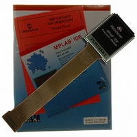
Manufacturer Part Number
PCM18XK1
Description
MODULE PROC PIC18F8680,6680,8565
Manufacturer
Microchip Technology
Datasheet
1.PCM18XK1.pdf
(496 pages)
Specifications of PCM18XK1
Accessory Type
Processor Module
Lead Free Status / RoHS Status
Not applicable / Not applicable
For Use With/related Products
ICE2000
For Use With
ICE2000 - EMULATOR MPLAB-ICE 2000 POD
Lead Free Status / Rohs Status
Lead free / RoHS Compliant


24.0
There are several features intended to maximize sys-
tem reliability, minimize cost through elimination of
external components, provide power saving operating
modes and offer code protection. These are:
• OSC Selection
• Reset
• Interrupts
• Watchdog Timer (WDT)
• Sleep
• Code Protection
• ID Locations
• In-Circuit Serial Programming
All PIC18F6585/8585/6680/8680 devices have a
Watchdog Timer which is permanently enabled via the
configuration bits or software controlled. It runs off its
own RC oscillator for added reliability. There are two
timers that offer necessary delays on power-up. One is
the Oscillator Start-up Timer (OST), intended to keep
the chip in Reset until the crystal oscillator is stable.
The other is the Power-up Timer (PWRT) which pro-
vides a fixed delay on power-up only, designed to keep
the part in Reset while the power supply stabilizes. With
these two timers on-chip, most applications need no
external Reset circuitry.
Sleep mode is designed to offer a very low current
Power-down mode. The user can wake-up from Sleep
through external Reset, Watchdog Timer Wake-up, or
through an interrupt. Several oscillator options are also
made available to allow the part to fit the application.
The RC oscillator option saves system cost, while the
LP crystal option saves power. A set of configuration
bits is used to select various options.
2004 Microchip Technology Inc.
- Power-on Reset (POR)
- Power-up Timer (PWRT)
- Oscillator Start-up Timer (OST)
- Brown-out Reset (BOR)
SPECIAL FEATURES OF THE
CPU
PIC18F6585/8585/6680/8680
24.1
The configuration bits can be programmed (read as ‘0’)
or left unprogrammed (read as ‘1’) to select various
device configurations. These bits are mapped, starting
at program memory location 300000h.
The user will note that address 300000h is beyond the
user program memory space. In fact, it belongs to the
configuration
3FFFFFh) which can only be accessed using table
reads and table writes.
Programming the Configuration registers is done in a
manner similar to programming the Flash memory. The
EECON1 register WR bit starts a self-timed write to the
Configuration register. In normal Operation mode, a
TBLWT instruction with the TBLPTR pointed to the Con-
figuration register sets up the address and the data for
the Configuration register write. Setting the WR bit
starts a long write to the Configuration register. The
Configuration registers are written a byte at a time. To
write or erase a configuration cell, a TBLWT instruction
can write a ‘1’ or a ‘0’ into the cell.
Configuration Bits
memory
space
(300000h
DS30491C-page 345
through
Related parts for PCM18XK1
Image
Part Number
Description
Manufacturer
Datasheet
Request
R

Part Number:
Description:
Manufacturer:
Microchip Technology Inc.
Datasheet:
Part Number:
Description:
Manufacturer:
Microchip Technology Inc.
Datasheet:
Part Number:
Description:
Manufacturer:
Microchip Technology Inc.
Datasheet:
Part Number:
Description:
Manufacturer:
Microchip Technology Inc.
Datasheet:
Part Number:
Description:
Manufacturer:
Microchip Technology Inc.
Datasheet:
Part Number:
Description:
Manufacturer:
Microchip Technology Inc.
Datasheet:
Part Number:
Description:
Manufacturer:
Microchip Technology Inc.
Datasheet:
Part Number:
Description:
Manufacturer:
Microchip Technology Inc.
Datasheet: