PCM18XK1 Microchip Technology, PCM18XK1 Datasheet - Page 15
PCM18XK1
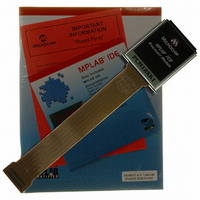
Manufacturer Part Number
PCM18XK1
Description
MODULE PROC PIC18F8680,6680,8565
Manufacturer
Microchip Technology
Datasheet
1.PCM18XK1.pdf
(496 pages)
Specifications of PCM18XK1
Accessory Type
Processor Module
Lead Free Status / RoHS Status
Not applicable / Not applicable
For Use With/related Products
ICE2000
For Use With
ICE2000 - EMULATOR MPLAB-ICE 2000 POD
Lead Free Status / Rohs Status
Lead free / RoHS Compliant


TABLE 1-2:
2004 Microchip Technology Inc.
RA0/AN0
RA1/AN1
RA2/AN2/V
RA3/AN3/V
RA4/T0CKI
RA5/AN4/LVDIN
RA6
Legend: TTL
Note 1:
RA0
AN0
RA1
AN1
RA2
AN2
V
RA3
AN3
V
RA4
T0CKI
RA5
AN4
LVDIN
REF
REF
2:
3:
4:
5:
6:
7:
Pin Name
-
+
ST
I
P
Alternate assignment for CCP2 in all operating modes except Microcontroller – applies to PIC18F8X8X only.
Default assignment when CCP2MX is set.
External memory interface functions are only available on PIC18F8X8X devices.
CCP2 is multiplexed with this pin by default when configured in Microcontroller mode; otherwise, it is
multiplexed with either RB3 or RC1.
PORTH and PORTJ are only available on PIC18F8X8X (80-pin) devices.
PSP is available in Microcontroller mode only.
On PIC18F8X8X devices, these pins can be multiplexed with RH7/RH6 by changing the ECCPMX
configuration bit.
REF
REF
-
+
PIC18F6585/8585/6680/8680 PINOUT I/O DESCRIPTIONS (CONTINUED)
= TTL compatible input
= Schmitt Trigger input with CMOS levels
= Input
= Power
TQFP PLCC
PIC18F6X8X PIC18F8X8X
24
23
22
21
28
27
Pin Number
34
33
32
31
39
38
PIC18F6585/8585/6680/8680
TQFP
30
29
28
27
34
33
Type
Pin
I/O
I/O
I/O
I/O
I/O
I/O
I
I
I
I
I
I
I
I
I
CMOS = CMOS compatible input or output
Analog = Analog input
O
OD
Analog
Analog
Analog
Analog
Analog
Analog
ST/OD
Analog
Analog
Buffer
Type
TTL
TTL
TTL
TTL
TTL
ST
= Output
= Open-Drain (no P diode to V
PORTA is a bidirectional I/O port.
Digital I/O.
Analog input 0.
Digital I/O.
Analog input 1.
Digital I/O.
Analog input 2.
A/D reference voltage (Low) input.
Digital I/O.
Analog input 3.
A/D reference voltage (High) input.
Digital I/O – Open-drain when
configured as output.
Timer0 external clock input.
Digital I/O.
Analog input 4.
Low-voltage detect input.
See the OSC2/CLKO/RA6 pin.
Description
DS30491C-page 13
DD
)
Related parts for PCM18XK1
Image
Part Number
Description
Manufacturer
Datasheet
Request
R

Part Number:
Description:
Manufacturer:
Microchip Technology Inc.
Datasheet:
Part Number:
Description:
Manufacturer:
Microchip Technology Inc.
Datasheet:
Part Number:
Description:
Manufacturer:
Microchip Technology Inc.
Datasheet:
Part Number:
Description:
Manufacturer:
Microchip Technology Inc.
Datasheet:
Part Number:
Description:
Manufacturer:
Microchip Technology Inc.
Datasheet:
Part Number:
Description:
Manufacturer:
Microchip Technology Inc.
Datasheet:
Part Number:
Description:
Manufacturer:
Microchip Technology Inc.
Datasheet:
Part Number:
Description:
Manufacturer:
Microchip Technology Inc.
Datasheet: