PCM18XK1 Microchip Technology, PCM18XK1 Datasheet - Page 233
PCM18XK1
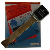
Manufacturer Part Number
PCM18XK1
Description
MODULE PROC PIC18F8680,6680,8565
Manufacturer
Microchip Technology
Datasheet
1.PCM18XK1.pdf
(496 pages)
Specifications of PCM18XK1
Accessory Type
Processor Module
Lead Free Status / RoHS Status
Not applicable / Not applicable
For Use With/related Products
ICE2000
For Use With
ICE2000 - EMULATOR MPLAB-ICE 2000 POD
Lead Free Status / Rohs Status
Lead free / RoHS Compliant


REGISTER 18-2:
2004 Microchip Technology Inc.
bit 7
bit 6
bit 5
bit 4
bit 3
bit 2
bit 1
bit 0
RCSTA: RECEIVE STATUS AND CONTROL REGISTER
bit 7
SPEN: Serial Port Enable bit
1 = Serial port enabled (configures RX/DT and TX/CK pins as serial port pins)
0 = Serial port disabled (held in Reset)
RX9: 9-bit Receive Enable bit
1 = Selects 9-bit reception
0 = Selects 8-bit reception
SREN: Single Receive Enable bit
Asynchronous mode:
Don’t care.
Synchronous mode – Master:
1 = Enables single receive
0 = Disables single receive
This bit is cleared after reception is complete.
Synchronous mode – Slave:
Don’t care.
CREN: Continuous Receive Enable bit
Asynchronous mode:
1 = Enables receiver
0 = Disables receiver
Synchronous mode:
1 = Enables continuous receive until enable bit CREN is cleared (CREN overrides SREN)
0 = Disables continuous receive
ADDEN: Address Detect Enable bit
Asynchronous mode 9-bit (RX9 = 1):
1 = Enables address detection, enables interrupt and loads the receive buffer when RSR<8>
0 = Disables address detection, all bytes are received and ninth bit can be used as parity bit
Asynchronous mode 9-bit (RX9 = 0):
Don’t care.
FERR: Framing Error bit
1 = Framing error (can be updated by reading RCREG register and receiving next valid byte)
0 = No framing error
OERR: Overrun Error bit
1 = Overrun error (can be cleared by clearing bit CREN)
0 = No overrun error
RX9D: 9th bit of Received Data
This can be an address/data bit or a parity bit and must be calculated by user firmware.
Legend:
R = Readable bit
- n = Value at POR
R/W-0
SPEN
is set
R/W-0
RX9
PIC18F6585/8585/6680/8680
R/W-0
SREN
W = Writable bit
‘1’ = Bit is set
R/W-0
CREN
ADDEN
R/W-0
U = Unimplemented bit, read as ‘0’
‘0’ = Bit is cleared
FERR
R-0
x = Bit is unknown
OERR
R-0
DS30491C-page 231
RX9D
R-x
bit 0
Related parts for PCM18XK1
Image
Part Number
Description
Manufacturer
Datasheet
Request
R

Part Number:
Description:
Manufacturer:
Microchip Technology Inc.
Datasheet:
Part Number:
Description:
Manufacturer:
Microchip Technology Inc.
Datasheet:
Part Number:
Description:
Manufacturer:
Microchip Technology Inc.
Datasheet:
Part Number:
Description:
Manufacturer:
Microchip Technology Inc.
Datasheet:
Part Number:
Description:
Manufacturer:
Microchip Technology Inc.
Datasheet:
Part Number:
Description:
Manufacturer:
Microchip Technology Inc.
Datasheet:
Part Number:
Description:
Manufacturer:
Microchip Technology Inc.
Datasheet:
Part Number:
Description:
Manufacturer:
Microchip Technology Inc.
Datasheet: