PCM18XK1 Microchip Technology, PCM18XK1 Datasheet - Page 30
PCM18XK1
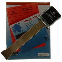
Manufacturer Part Number
PCM18XK1
Description
MODULE PROC PIC18F8680,6680,8565
Manufacturer
Microchip Technology
Datasheet
1.PCM18XK1.pdf
(496 pages)
Specifications of PCM18XK1
Accessory Type
Processor Module
Lead Free Status / RoHS Status
Not applicable / Not applicable
For Use With/related Products
ICE2000
For Use With
ICE2000 - EMULATOR MPLAB-ICE 2000 POD
Lead Free Status / Rohs Status
Lead free / RoHS Compliant


PIC18F6585/8585/6680/8680
2.6.2
PIC18F6585/8585/6680/8680 devices contain circuitry
to prevent “glitches” when switching between oscillator
sources. Essentially, the circuitry waits for eight rising
edges of the clock source that the processor is switch-
ing to. This ensures that the new clock source is stable
and that its pulse width will not be less than the shortest
pulse width of the two clock sources.
A timing diagram, indicating the transition from the
main oscillator to the Timer1 oscillator, is shown in
Figure 2-8. The Timer1 oscillator is assumed to be run-
ning all the time. After the SCS0 bit is set, the processor
is frozen at the next occurring Q1 cycle. After eight
synchronization cycles are counted from the Timer1
oscillator, operation resumes. No additional delays are
required after the synchronization cycles.
FIGURE 2-8:
FIGURE 2-9:
DS30491C-page 28
(OSCCON<0>)
Note:
System Clock
T1OSI
OSC1
Internal
System
Clock
SCS
(OSCCON<0>)
Program
Counter
Note:
Program
Counter
Internal
T1OSI
OSC1
SCS
T
OSCILLATOR TRANSITIONS
T
OST
Q1
DLY
T
= 1024 T
Q2
OSC
is the delay from SCS high to first count of transition circuit.
Q3
PC
Q3
PC
OSC
Q4
TIMING DIAGRAM FOR TRANSITION FROM OSC1 TO TIMER1 OSCILLATOR
TIMING FOR TRANSITION BETWEEN TIMER1 AND OSC1 (HS, XT, LP)
Q4
(drawing not to scale).
Q1
T
DLY
1
Q1
2
T
T
1
P
3
T
OST
4
T
SCS
PC + 2
T
5
OSC
6
PC + 2
The sequence of events that takes place when switch-
ing from the Timer1 oscillator to the main oscillator will
depend on the mode of the main oscillator. In addition
to eight clock cycles of the main oscillator, additional
delays may take place.
If the main oscillator is configured for an external
crystal (HS, XT, LP), then the transition will take place
after an oscillator start-up time (T
timing diagram, indicating the transition from the
Timer1 oscillator to the main oscillator for HS, XT and
LP modes, is shown in Figure 2-9.
7
1
2
8
Q1
3
Q2
4
T
T
SCS
T
1
P
5
Q3
6
Q4
2004 Microchip Technology Inc.
7
Q1
8
Q1
Q2 Q3
Q2
OST
PC + 4
) has occurred. A
Q4
Q3
Q1 Q2
Q4
PC + 6
Q1
Q3
Related parts for PCM18XK1
Image
Part Number
Description
Manufacturer
Datasheet
Request
R

Part Number:
Description:
Manufacturer:
Microchip Technology Inc.
Datasheet:
Part Number:
Description:
Manufacturer:
Microchip Technology Inc.
Datasheet:
Part Number:
Description:
Manufacturer:
Microchip Technology Inc.
Datasheet:
Part Number:
Description:
Manufacturer:
Microchip Technology Inc.
Datasheet:
Part Number:
Description:
Manufacturer:
Microchip Technology Inc.
Datasheet:
Part Number:
Description:
Manufacturer:
Microchip Technology Inc.
Datasheet:
Part Number:
Description:
Manufacturer:
Microchip Technology Inc.
Datasheet:
Part Number:
Description:
Manufacturer:
Microchip Technology Inc.
Datasheet: