PCM18XK1 Microchip Technology, PCM18XK1 Datasheet - Page 246
PCM18XK1
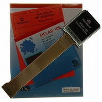
Manufacturer Part Number
PCM18XK1
Description
MODULE PROC PIC18F8680,6680,8565
Manufacturer
Microchip Technology
Datasheet
1.PCM18XK1.pdf
(496 pages)
Specifications of PCM18XK1
Accessory Type
Processor Module
Lead Free Status / RoHS Status
Not applicable / Not applicable
For Use With/related Products
ICE2000
For Use With
ICE2000 - EMULATOR MPLAB-ICE 2000 POD
Lead Free Status / Rohs Status
Lead free / RoHS Compliant


PIC18F6585/8585/6680/8680
18.3
The Synchronous Master mode is entered by setting
the CSRC bit (TXSTA<7>). In this mode, the data is
transmitted in a half-duplex manner (i.e., transmission
and reception do not occur at the same time). When
transmitting data, the reception is inhibited and vice
versa. Synchronous mode is entered by setting bit
SYNC (TXSTA<4>). In addition, enable bit, SPEN
(RCSTA<7>), is set in order to configure the
RC6/TX/CK and RC7/RX/DT I/O pins to CK (clock) and
DT (data) lines, respectively.
The Master mode indicates that the processor trans-
mits the master clock on the CK line. Clock polarity is
selected with the SCKP bit (BAUDCON<5>); setting
SCKP sets the Idle state on CK as high, while clearing
the bit sets the Idle state as low. This option is provided
to support Microwire devices with this module.
18.3.1
The USART transmitter block diagram is shown in
Figure 18-2. The heart of the transmitter is the Transmit
(Serial) Shift Register (TSR). The Shift register obtains
its data from the Read/Write Transmit Buffer register,
TXREG. The TXREG register is loaded with data in
software. The TSR register is not loaded until the last
bit has been transmitted from the previous load. As
soon as the last bit is transmitted, the TSR is loaded
with new data from the TXREG (if available).
FIGURE 18-10:
DS30491C-page 244
(Interrupt Flag)
Note:
TXREG Reg
RC7/RX/DT
RC6/TX/CK
RC6/TX/CK
(SCKP = 0)
(SCKP = 1)
TRMT bit
TXEN bit
TXIF bit
Write to
Sync Master mode, SPBRG = 0, continuous transmission of two 8-bit words.
USART Synchronous
Master Mode
pin
pin
pin
USART SYNCHRONOUS MASTER
TRANSMISSION
Q1 Q2 Q3Q4 Q1 Q2 Q3 Q4 Q1 Q2 Q3 Q4 Q1Q2 Q3 Q4 Q1 Q2 Q3 Q4
‘1’
Write Word 1
SYNCHRONOUS TRANSMISSION
bit 0
Write Word 2
bit 1
Word 1
bit 2
Q3 Q4 Q1 Q2 Q3 Q4 Q1Q2 Q3 Q4 Q1 Q2 Q3 Q4 Q1 Q2 Q3 Q4 Q1 Q2 Q3 Q4 Q1 Q2 Q3 Q4
Once the TXREG register transfers the data to the TSR
register (occurs in one T
and interrupt bit TXIF (PIR1<4>) is set. The interrupt
can be enabled/disabled by setting/clearing enable bit,
TXIE (PIE1<4>). Flag bit TXIF will be set regardless of
the state of enable bit TXIE and cannot be cleared in
software. It will reset only when new data is loaded into
the TXREG register.
While flag bit TXIF indicates the status of the TXREG
register, another bit, TRMT (TXSTA<1>), shows the sta-
tus of the TSR register. TRMT is a read-only bit which is
set when the TSR is empty. No interrupt logic is tied to
this bit so the user must poll this bit in order to determine
if the TSR register is empty. The TSR is not mapped in
data memory so it is not available to the user.
To set up a synchronous master transmission:
1.
2.
3.
4.
5.
6.
7.
8.
bit 7
Initialize the SPBRGH:SPBRG registers for the
appropriate baud rate. Set or clear the BRGH
and BRG16 bits, as required, to achieve the
desired baud rate.
Enable the synchronous master serial port by
setting bits SYNC, SPEN and CSRC.
If interrupts are desired, set enable bit TXIE.
If 9-bit transmission is desired, set bit TX9.
Enable the transmission by setting bit TXEN.
If 9-bit transmission is selected, the ninth bit
should be loaded in bit TX9D.
Start transmission by loading data to the TXREG
register.
If using interrupts, ensure that the GIE and PEIE
bits in the INTCON register (INTCON<7:6>) are
set.
bit 0
Word 2
bit 1
2004 Microchip Technology Inc.
CYCLE
), the TXREG is empty
bit 7
‘1’
Related parts for PCM18XK1
Image
Part Number
Description
Manufacturer
Datasheet
Request
R

Part Number:
Description:
Manufacturer:
Microchip Technology Inc.
Datasheet:
Part Number:
Description:
Manufacturer:
Microchip Technology Inc.
Datasheet:
Part Number:
Description:
Manufacturer:
Microchip Technology Inc.
Datasheet:
Part Number:
Description:
Manufacturer:
Microchip Technology Inc.
Datasheet:
Part Number:
Description:
Manufacturer:
Microchip Technology Inc.
Datasheet:
Part Number:
Description:
Manufacturer:
Microchip Technology Inc.
Datasheet:
Part Number:
Description:
Manufacturer:
Microchip Technology Inc.
Datasheet:
Part Number:
Description:
Manufacturer:
Microchip Technology Inc.
Datasheet: