PCM18XK1 Microchip Technology, PCM18XK1 Datasheet - Page 268
PCM18XK1
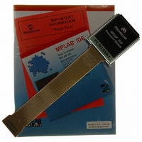
Manufacturer Part Number
PCM18XK1
Description
MODULE PROC PIC18F8680,6680,8565
Manufacturer
Microchip Technology
Datasheet
1.PCM18XK1.pdf
(496 pages)
Specifications of PCM18XK1
Accessory Type
Processor Module
Lead Free Status / RoHS Status
Not applicable / Not applicable
For Use With/related Products
ICE2000
For Use With
ICE2000 - EMULATOR MPLAB-ICE 2000 POD
Lead Free Status / Rohs Status
Lead free / RoHS Compliant


PIC18F6585/8585/6680/8680
FIGURE 21-1:
21.2
The full range of voltage reference cannot be realized
due to the construction of the module. The transistors
on the top and bottom of the resistor ladder network
(Figure 21-1) keep CV
ence source rails. The voltage reference is derived
from the reference source; therefore, the CV
changes with fluctuations in that source. The tested
absolute accuracy of the voltage reference can be
found in Section 27.0 “Electrical Characteristics”.
21.3
When the device wakes up from Sleep through an
interrupt or a Watchdog Timer time-out, the contents of
the CVRCON register are not affected. To minimize
current consumption in Sleep mode, the voltage
reference should be disabled.
DS30491C-page 266
CVREN
Note: R is defined in Section 27.0 “Electrical Characteristics”.
Voltage Reference Accuracy/Error
Operation During Sleep
CVRSS = 0
CV
REF
V
DD
REF
VOLTAGE REFERENCE BLOCK DIAGRAM
V
from approaching the refer-
REF
CVRSS = 1
+
8R
R
REF
output
R
16 Stages
16-1 Analog Mux
21.4
A device Reset disables the voltage reference by
clearing bit CVREN (CVRCON<7>). This Reset also
disconnects the reference from the RA2 pin by clearing
bit CVROE (CVRCON<6>) and selects the high-
voltage range by clearing bit CVRR (CVRCON<5>).
The VRSS value select bits, CVRCON<3:0>, are also
cleared.
21.5
The voltage reference module operates independently
of the comparator module. The output of the reference
generator may be connected to the RF5 pin if the
TRISF<5> bit is set and the CVROE bit is set. Enabling
the voltage reference output onto the RF5 pin with an
input signal present will increase current consumption.
Connecting RF5 as a digital output with VRSS enabled
will also increase current consumption.
The RF5 pin can be used as a simple D/A output with
limited drive capability. Due to the limited current drive
capability, a buffer must be used on the voltage refer-
ence output for external connections to V
Figure 21-2 shows an example buffering technique.
R
Effects of a Reset
Connection Considerations
R
2004 Microchip Technology Inc.
8R
CVR3
CVR0
(From CVRCON<3:0>)
CVRR
CVRSS = 0
CVRSS = 1
V
REF
-
REF
.
Related parts for PCM18XK1
Image
Part Number
Description
Manufacturer
Datasheet
Request
R

Part Number:
Description:
Manufacturer:
Microchip Technology Inc.
Datasheet:
Part Number:
Description:
Manufacturer:
Microchip Technology Inc.
Datasheet:
Part Number:
Description:
Manufacturer:
Microchip Technology Inc.
Datasheet:
Part Number:
Description:
Manufacturer:
Microchip Technology Inc.
Datasheet:
Part Number:
Description:
Manufacturer:
Microchip Technology Inc.
Datasheet:
Part Number:
Description:
Manufacturer:
Microchip Technology Inc.
Datasheet:
Part Number:
Description:
Manufacturer:
Microchip Technology Inc.
Datasheet:
Part Number:
Description:
Manufacturer:
Microchip Technology Inc.
Datasheet: