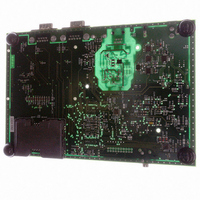
AT91RM3400-DK Atmel, AT91RM3400-DK Datasheet - Page 54

AT91RM3400-DK
Manufacturer Part Number
AT91RM3400-DK
Description
KIT DEV FOR AT91RM3400
Manufacturer
Atmel
Series
AT91SAM Smart ARMr
Type
MCUr
Datasheets
1.AT91RM3400-DK.pdf
(461 pages)
2.AT91RM3400-DK.pdf
(2 pages)
3.AT91RM3400-DK.pdf
(25 pages)
Specifications of AT91RM3400-DK
Contents
Evaluation Board, Software and Documentation
Processor To Be Evaluated
AT91RM3400
Data Bus Width
32 bit
Interface Type
RS-232, USB
For Use With/related Products
AT91RM3400
Lead Free Status / RoHS Status
Contains lead / RoHS non-compliant
- Current page: 54 of 461
- Download datasheet (6Mb)
Hardware and
Software
Constraints
54
AT91RM3400
The software limitations of the Boot Program are:
•
•
•
•
The hardware limitations of the Boot Program are:
•
•
The SPI and TWI drivers use several PIOs in alternate functions to communicate with devices.
Care must be taken when these PIOs are used by the application. The devices connected
could be unintentionally driven at boot time, and electrical conflicts between SPI or TWI output
pins and the connected devices may appear.
To assure correct functionality, it is recommended to plug in critical devices to other pins or to
boot on an external 16-bit parallel memory (if product integrates an EBI) by setting bit BMS.
Table 15 contains a list of pins that are driven during the Boot Program execution. These pins
are driven during the boot sequence for a period of about 6 ms if no correct boot program is
found. The download through the TWI takes about 5 sec for 64K bytes due to the TWI bit rate
(100 Kbits/s).
For the DataFlash driven by SPCK signal at 12 MHz, the time to download 64K bytes is
reduced to 66 ms.
Before performing the jump to the application in internal SRAM, all the PIOs and peripherals
used in the Boot Program are set to their reset state.
Table 15. Pins Driven during Boot Program Execution
Note:
Pin Used
MOSI
SPCK
NPCS0
TWD
TWCK
The downloaded code size is less than the SRAM size embedded in the product.
The device address of the EEPROM must be 0 on the TWI bus.
The code is always downloaded from the device address 0x0000_0000 (DataFlash,
EEPROM) to the address 0x0000_0000 of the internal SRAM (after remap).
The downloaded code must be position-independent or linked at address 0x0000_0000.
The DataFlash must be connected to NPCS0 of the SPI.
The 8-bit parallel Flash must be connected to NCS0 of the EBI if the device integrates an
EBI.
(1)
(1)
(1)
(1)
(1)
1. See “Peripheral Multiplexing on PIO Lines” on page 13.
SPI (Dataflash)
O
O
O
X
X
TWI (EEPROM)
I/O
O
X
X
X
1790A–ATARM–11/03
Related parts for AT91RM3400-DK
Image
Part Number
Description
Manufacturer
Datasheet
Request
R

Part Number:
Description:
DEV KIT FOR AVR/AVR32
Manufacturer:
Atmel
Datasheet:

Part Number:
Description:
INTERVAL AND WIPE/WASH WIPER CONTROL IC WITH DELAY
Manufacturer:
ATMEL Corporation
Datasheet:

Part Number:
Description:
Low-Voltage Voice-Switched IC for Hands-Free Operation
Manufacturer:
ATMEL Corporation
Datasheet:

Part Number:
Description:
MONOLITHIC INTEGRATED FEATUREPHONE CIRCUIT
Manufacturer:
ATMEL Corporation
Datasheet:

Part Number:
Description:
AM-FM Receiver IC U4255BM-M
Manufacturer:
ATMEL Corporation
Datasheet:

Part Number:
Description:
Monolithic Integrated Feature Phone Circuit
Manufacturer:
ATMEL Corporation
Datasheet:

Part Number:
Description:
Multistandard Video-IF and Quasi Parallel Sound Processing
Manufacturer:
ATMEL Corporation
Datasheet:

Part Number:
Description:
High-performance EE PLD
Manufacturer:
ATMEL Corporation
Datasheet:

Part Number:
Description:
8-bit Flash Microcontroller
Manufacturer:
ATMEL Corporation
Datasheet:

Part Number:
Description:
2-Wire Serial EEPROM
Manufacturer:
ATMEL Corporation
Datasheet:


