C8051F700DK Silicon Laboratories Inc, C8051F700DK Datasheet - Page 10
C8051F700DK
Manufacturer Part Number
C8051F700DK
Description
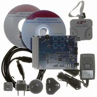
DEV KIT FOR C8051F700
Manufacturer
Silicon Laboratories Inc
Type
MCUr
Datasheets
1.C8051F700-TB.pdf
(1 pages)
2.C8051F700-TB.pdf
(306 pages)
3.C8051F700-TB.pdf
(18 pages)
Specifications of C8051F700DK
Contents
Board, Cables, CD, Debugger, Power Supply
Processor To Be Evaluated
C8051F7x
Processor Series
C8051F7xx
Interface Type
USB
Operating Supply Voltage
3.3 V
Lead Free Status / RoHS Status
Lead free / RoHS Compliant
For Use With/related Products
C8051F7xx
Lead Free Status / Rohs Status
Lead free / RoHS Compliant
Other names
336-1635


C8051F70x/71x
10
Figure 32.6. UART Multi-Processor Mode Interconnect Diagram ......................... 258
Figure 33.1. T0 Mode 0 Block Diagram ................................................................. 265
Figure 33.2. T0 Mode 2 Block Diagram ................................................................. 266
Figure 33.3. T0 Mode 3 Block Diagram ................................................................. 267
Figure 33.4. Timer 2 16-Bit Mode Block Diagram ................................................. 272
Figure 33.5. Timer 2 8-Bit Mode Block Diagram ................................................... 273
Figure 33.7. Timer 3 16-Bit Mode Block Diagram ................................................. 278
Figure 33.8. Timer 3 8-Bit Mode Block Diagram ................................................... 279
Figure 33.9. Timer 3 Capture Mode Block Diagram .............................................. 280
Figure 34.1. PCA Block Diagram ........................................................................... 284
Figure 34.2. PCA Counter/Timer Block Diagram ................................................... 285
Figure 34.3. PCA Interrupt Block Diagram ............................................................ 286
Figure 34.4. PCA Capture Mode Diagram ............................................................. 288
Figure 34.5. PCA Software Timer Mode Diagram ................................................. 289
Figure 34.6. PCA High-Speed Output Mode Diagram ........................................... 290
Figure 34.7. PCA Frequency Output Mode ........................................................... 291
Figure 34.8. PCA 8-Bit PWM Mode Diagram ........................................................ 292
Figure 34.9. PCA 9, 10 and 11-Bit PWM Mode Diagram ...................................... 293
Figure 34.10. PCA 16-Bit PWM Mode ................................................................... 294
Figure 35.1. Typical C2CK Pin Sharing ................................................................. 304
Rev. 1.0
Related parts for C8051F700DK
Image
Part Number
Description
Manufacturer
Datasheet
Request
R

Part Number:
Description:
SMD/C°/SINGLE-ENDED OUTPUT SILICON OSCILLATOR
Manufacturer:
Silicon Laboratories Inc
Part Number:
Description:
Manufacturer:
Silicon Laboratories Inc
Datasheet:
Part Number:
Description:
N/A N/A/SI4010 AES KEYFOB DEMO WITH LCD RX
Manufacturer:
Silicon Laboratories Inc
Datasheet:
Part Number:
Description:
N/A N/A/SI4010 SIMPLIFIED KEY FOB DEMO WITH LED RX
Manufacturer:
Silicon Laboratories Inc
Datasheet:
Part Number:
Description:
N/A/-40 TO 85 OC/EZLINK MODULE; F930/4432 HIGH BAND (REV E/B1)
Manufacturer:
Silicon Laboratories Inc
Part Number:
Description:
EZLink Module; F930/4432 Low Band (rev e/B1)
Manufacturer:
Silicon Laboratories Inc
Part Number:
Description:
I°/4460 10 DBM RADIO TEST CARD 434 MHZ
Manufacturer:
Silicon Laboratories Inc
Part Number:
Description:
I°/4461 14 DBM RADIO TEST CARD 868 MHZ
Manufacturer:
Silicon Laboratories Inc
Part Number:
Description:
I°/4463 20 DBM RFSWITCH RADIO TEST CARD 460 MHZ
Manufacturer:
Silicon Laboratories Inc
Part Number:
Description:
I°/4463 20 DBM RADIO TEST CARD 868 MHZ
Manufacturer:
Silicon Laboratories Inc
Part Number:
Description:
I°/4463 27 DBM RADIO TEST CARD 868 MHZ
Manufacturer:
Silicon Laboratories Inc
Part Number:
Description:
I°/4463 SKYWORKS 30 DBM RADIO TEST CARD 915 MHZ
Manufacturer:
Silicon Laboratories Inc
Part Number:
Description:
N/A N/A/-40 TO 85 OC/4463 RFMD 30 DBM RADIO TEST CARD 915 MHZ
Manufacturer:
Silicon Laboratories Inc
Part Number:
Description:
I°/4463 20 DBM RADIO TEST CARD 169 MHZ
Manufacturer:
Silicon Laboratories Inc