C8051F700DK Silicon Laboratories Inc, C8051F700DK Datasheet - Page 8
C8051F700DK
Manufacturer Part Number
C8051F700DK
Description
DEV KIT FOR C8051F700
Manufacturer
Silicon Laboratories Inc
Type
MCUr
Datasheets
1.C8051F700-TB.pdf
(1 pages)
2.C8051F700-TB.pdf
(306 pages)
3.C8051F700-TB.pdf
(18 pages)
Specifications of C8051F700DK
Contents
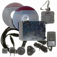
Board, Cables, CD, Debugger, Power Supply
Processor To Be Evaluated
C8051F7x
Processor Series
C8051F7xx
Interface Type
USB
Operating Supply Voltage
3.3 V
Lead Free Status / RoHS Status
Lead free / RoHS Compliant
For Use With/related Products
C8051F7xx
Lead Free Status / Rohs Status
Lead free / RoHS Compliant
Other names
336-1635


C8051F70x/71x
List of Figures
8
Figure 1.1. C8051F700/1 Block Diagram ................................................................ 18
Figure 1.2. C8051F702/3 Block Diagram ................................................................ 19
Figure 1.3. C8051F704/5 Block Diagram ................................................................ 20
Figure 1.4. C8051F706/07 Block Diagram .............................................................. 21
Figure 1.5. C8051F708/09/10/11 Block Diagram .................................................... 22
Figure 1.6. C8051F712/13/14/15 Block Diagram .................................................... 23
Figure 1.7. C8051F716 Block Diagram ................................................................... 24
Figure 1.8. C8051F717 Block Diagram ................................................................... 25
Figure 3.1. C8051F7xx-GQ TQFP64 Pinout Diagram (Top View) .......................... 32
Figure 3.2. C8051F7xx-GQ QFP48 Pinout Diagram (Top View) ............................. 33
Figure 3.3. C8051F7xx-GM QFN48 Pinout Diagram (Top View) ............................ 34
Figure 3.4. C8051F716-GM QFN32 Pinout Diagram (Top View) ............................ 35
Figure 3.5. C8051F717-GM QFN24 Pinout Diagram (Top View) ............................ 36
Figure 4.1. TQFP-64 Package Drawing .................................................................. 37
Figure 4.2. TQFP-64 PCB Land Pattern .................................................................. 38
Figure 5.1. TQFP-48 Package Drawing .................................................................. 39
Figure 5.2. TQFP-48 PCB Land Pattern .................................................................. 40
Figure 6.1. QFN-48 Package Drawing .................................................................... 41
Figure 6.2. QFN-48 PCB Land Pattern .................................................................... 42
Figure 7.1. QFN-32 Package Drawing .................................................................... 43
Figure 7.2. QFN-32 Recommended PCB Land Pattern .......................................... 44
Figure 8.1. QFN-24 Package Drawing .................................................................... 45
Figure 8.2. QFN-24 Recommended PCB Land Pattern .......................................... 46
Figure 10.1. ADC0 Functional Block Diagram ......................................................... 55
Figure 10.2. 10-Bit ADC Track and Conversion Example Timing ........................... 57
Figure 10.3. ADC0 Equivalent Input Circuits ........................................................... 58
Figure 10.4. ADC Window Compare Example: Right-Justified Data ....................... 64
Figure 10.5. ADC Window Compare Example: Left-Justified Data ......................... 64
Figure 10.6. ADC0 Multiplexer Block Diagram ........................................................ 65
Figure 11.1. Temperature Sensor Transfer Function .............................................. 67
Figure 11.2. Temperature Sensor Error with 1-Point Calibration at 0 Celsius ......... 68
Figure 12.1. Voltage Reference Functional Block Diagram ..................................... 69
Figure 14.1. Comparator0 Functional Block Diagram ............................................. 74
Figure 14.2. Comparator Hysteresis Plot ................................................................ 75
Figure 14.3. Comparator Input Multiplexer Block Diagram ...................................... 78
Figure 15.1. CS0 Block Diagram ............................................................................. 80
Figure 15.2. Auto-Scan Example ............................................................................. 83
Figure 15.3. CS0 Multiplexer Block Diagram ........................................................... 96
Figure 16.1. CIP-51 Block Diagram ......................................................................... 98
Figure 17.1. C8051F70x/71x Memory Map ........................................................... 108
Figure 17.2. Flash Program Memory Map ............................................................. 109
Figure 18.1. Multiplexed Configuration Example ................................................... 115
Figure 18.2. Non-multiplexed Configuration Example ........................................... 116
Rev. 1.0
Related parts for C8051F700DK
Image
Part Number
Description
Manufacturer
Datasheet
Request
R

Part Number:
Description:
SMD/C°/SINGLE-ENDED OUTPUT SILICON OSCILLATOR
Manufacturer:
Silicon Laboratories Inc
Part Number:
Description:
Manufacturer:
Silicon Laboratories Inc
Datasheet:
Part Number:
Description:
N/A N/A/SI4010 AES KEYFOB DEMO WITH LCD RX
Manufacturer:
Silicon Laboratories Inc
Datasheet:
Part Number:
Description:
N/A N/A/SI4010 SIMPLIFIED KEY FOB DEMO WITH LED RX
Manufacturer:
Silicon Laboratories Inc
Datasheet:
Part Number:
Description:
N/A/-40 TO 85 OC/EZLINK MODULE; F930/4432 HIGH BAND (REV E/B1)
Manufacturer:
Silicon Laboratories Inc
Part Number:
Description:
EZLink Module; F930/4432 Low Band (rev e/B1)
Manufacturer:
Silicon Laboratories Inc
Part Number:
Description:
I°/4460 10 DBM RADIO TEST CARD 434 MHZ
Manufacturer:
Silicon Laboratories Inc
Part Number:
Description:
I°/4461 14 DBM RADIO TEST CARD 868 MHZ
Manufacturer:
Silicon Laboratories Inc
Part Number:
Description:
I°/4463 20 DBM RFSWITCH RADIO TEST CARD 460 MHZ
Manufacturer:
Silicon Laboratories Inc
Part Number:
Description:
I°/4463 20 DBM RADIO TEST CARD 868 MHZ
Manufacturer:
Silicon Laboratories Inc
Part Number:
Description:
I°/4463 27 DBM RADIO TEST CARD 868 MHZ
Manufacturer:
Silicon Laboratories Inc
Part Number:
Description:
I°/4463 SKYWORKS 30 DBM RADIO TEST CARD 915 MHZ
Manufacturer:
Silicon Laboratories Inc
Part Number:
Description:
N/A N/A/-40 TO 85 OC/4463 RFMD 30 DBM RADIO TEST CARD 915 MHZ
Manufacturer:
Silicon Laboratories Inc
Part Number:
Description:
I°/4463 20 DBM RADIO TEST CARD 169 MHZ
Manufacturer:
Silicon Laboratories Inc