C8051F700DK Silicon Laboratories Inc, C8051F700DK Datasheet - Page 81
C8051F700DK
Manufacturer Part Number
C8051F700DK
Description
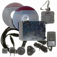
DEV KIT FOR C8051F700
Manufacturer
Silicon Laboratories Inc
Type
MCUr
Datasheets
1.C8051F700-TB.pdf
(1 pages)
2.C8051F700-TB.pdf
(306 pages)
3.C8051F700-TB.pdf
(18 pages)
Specifications of C8051F700DK
Contents
Board, Cables, CD, Debugger, Power Supply
Processor To Be Evaluated
C8051F7x
Processor Series
C8051F7xx
Interface Type
USB
Operating Supply Voltage
3.3 V
Lead Free Status / RoHS Status
Lead free / RoHS Compliant
For Use With/related Products
C8051F7xx
Lead Free Status / Rohs Status
Lead free / RoHS Compliant
Other names
336-1635


15.1. Configuring Port Pins as Capacitive Sense Inputs
In order for a port pin to be measured by CS0, that port pin must be configured as an analog input (see “28.
Port Input/Output” ). Configuring the input multiplexer to a port pin not configured as an analog input will
cause the capacitance-to-digital converter to output incorrect measurements.
Note: When CS0 begins a conversion to measure capacitance on a port pin, CS0 grounds all other port pins that
15.2. CS0 Gain Adjustment
The gain of the CS0 circuit can be adjusted in integer increments from 1x to 8x (8x is the default). High
gain gives the best sensitivity and resolution for small capacitors, such as those typically implemented as
touch-sensitive PCB features. To measure larger capacitance values, the gain can be lowered. However,
lower gain values will affect the overall conversion time. SeeTable 15.1 for more details on the gain adjust-
ment. The bits CS0CG[2:0] in register CS0MD1 set the gain value.
15.3. Capacitive Sense Start-Of-Conversion Sources
A capacitive sense conversion can be initiated in one of seven ways, depending on the programmed state
of the CS0 start of conversion bits (CS0CF6:4). Conversions may be initiated by one of the following:
1. Writing a 1 to the CS0BUSY bit of register CS0CN
2. Timer 0 overflow
3. Timer 2 overflow
4. Timer 1 overflow
5. Timer 3 overflow
6. Convert continuously
7. Convert continuously with auto-scan enabled
Notes:
CS0CG[2:0] (Gain)
1. The maximum total capacitance values listed in this table are for guidance only, and are not a specification.
2. Conversion times are nominal, and listed for 13-bit conversions with all other CS0 settings at their default
meet the following requirements:
- The port pin is accessible by the CS0 input multiplexer.
- The port pin is configured as an analog input.
- The port latch contains a 0.
The total measured capacitance will include internal capacitance as well as external parasitics, and the actual
external capacitance being measured. Please refer to the Electrical Specifications for details on the maximum
external capacitance.
values.
000b (1x)
001b (2x)
010b (3x)
011b (4x)
100b (5x)
101b (6x)
110b (7x)
111b (8x)
Table 15.1. Gain Setting vs. Maximum Capacitance and Conversion Time
Maximum Total Capacitance (pF)
520
260
175
130
105
85
75
65
Rev. 1.0
1
C8051F70x/71x
Conversion Time (µs)
178
93
66
52
43
38
34
31
2
81
Related parts for C8051F700DK
Image
Part Number
Description
Manufacturer
Datasheet
Request
R

Part Number:
Description:
SMD/C°/SINGLE-ENDED OUTPUT SILICON OSCILLATOR
Manufacturer:
Silicon Laboratories Inc
Part Number:
Description:
Manufacturer:
Silicon Laboratories Inc
Datasheet:
Part Number:
Description:
N/A N/A/SI4010 AES KEYFOB DEMO WITH LCD RX
Manufacturer:
Silicon Laboratories Inc
Datasheet:
Part Number:
Description:
N/A N/A/SI4010 SIMPLIFIED KEY FOB DEMO WITH LED RX
Manufacturer:
Silicon Laboratories Inc
Datasheet:
Part Number:
Description:
N/A/-40 TO 85 OC/EZLINK MODULE; F930/4432 HIGH BAND (REV E/B1)
Manufacturer:
Silicon Laboratories Inc
Part Number:
Description:
EZLink Module; F930/4432 Low Band (rev e/B1)
Manufacturer:
Silicon Laboratories Inc
Part Number:
Description:
I°/4460 10 DBM RADIO TEST CARD 434 MHZ
Manufacturer:
Silicon Laboratories Inc
Part Number:
Description:
I°/4461 14 DBM RADIO TEST CARD 868 MHZ
Manufacturer:
Silicon Laboratories Inc
Part Number:
Description:
I°/4463 20 DBM RFSWITCH RADIO TEST CARD 460 MHZ
Manufacturer:
Silicon Laboratories Inc
Part Number:
Description:
I°/4463 20 DBM RADIO TEST CARD 868 MHZ
Manufacturer:
Silicon Laboratories Inc
Part Number:
Description:
I°/4463 27 DBM RADIO TEST CARD 868 MHZ
Manufacturer:
Silicon Laboratories Inc
Part Number:
Description:
I°/4463 SKYWORKS 30 DBM RADIO TEST CARD 915 MHZ
Manufacturer:
Silicon Laboratories Inc
Part Number:
Description:
N/A N/A/-40 TO 85 OC/4463 RFMD 30 DBM RADIO TEST CARD 915 MHZ
Manufacturer:
Silicon Laboratories Inc
Part Number:
Description:
I°/4463 20 DBM RADIO TEST CARD 169 MHZ
Manufacturer:
Silicon Laboratories Inc