C8051F700DK Silicon Laboratories Inc, C8051F700DK Datasheet - Page 244
C8051F700DK
Manufacturer Part Number
C8051F700DK
Description
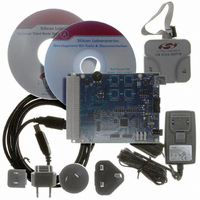
DEV KIT FOR C8051F700
Manufacturer
Silicon Laboratories Inc
Type
MCUr
Datasheets
1.C8051F700-TB.pdf
(1 pages)
2.C8051F700-TB.pdf
(306 pages)
3.C8051F700-TB.pdf
(18 pages)
Specifications of C8051F700DK
Contents
Board, Cables, CD, Debugger, Power Supply
Processor To Be Evaluated
C8051F7x
Processor Series
C8051F7xx
Interface Type
USB
Operating Supply Voltage
3.3 V
Lead Free Status / RoHS Status
Lead free / RoHS Compliant
For Use With/related Products
C8051F7xx
Lead Free Status / Rohs Status
Lead free / RoHS Compliant
Other names
336-1635


C8051F70x/71x
31.3. SPI0 Slave Mode Operation
When SPI0 is enabled and not configured as a master, it will operate as a SPI slave. As a slave, bytes are
shifted in through the MOSI pin and out through the MISO pin by a master device controlling the SCK sig-
nal. A bit counter in the SPI0 logic counts SCK edges. When 8 bits have been shifted through the shift reg-
ister, the SPIF flag is set to logic 1, and the byte is copied into the receive buffer. Data is read from the
receive buffer by reading SPI0DAT. A slave device cannot initiate transfers. Data to be transferred to the
master device is pre-loaded into the shift register by writing to SPI0DAT. Writes to SPI0DAT are double-
buffered, and are placed in the transmit buffer first. If the shift register is empty, the contents of the transmit
buffer will immediately be transferred into the shift register. When the shift register already contains data,
the SPI will load the shift register with the transmit buffer’s contents after the last SCK edge of the next (or
current) SPI transfer.
When configured as a slave, SPI0 can be configured for 4-wire or 3-wire operation. The default, 4-wire
slave mode, is active when NSSMD1 (SPI0CN.3) = 0 and NSSMD0 (SPI0CN.2) = 1. In 4-wire mode, the
NSS signal is routed to a port pin and configured as a digital input. SPI0 is enabled when NSS is logic 0,
and disabled when NSS is logic 1. The bit counter is reset on a falling edge of NSS. The NSS signal must
be driven low at least 2 system clocks before the first active edge of SCK for each byte transfer.
Figure 31.4 shows a connection diagram between two slave devices in 4-wire slave mode and a master
device.
3-wire slave mode is active when NSSMD1 (SPI0CN.3) = 0 and NSSMD0 (SPI0CN.2) = 0. NSS is not
used in this mode, and is not mapped to an external port pin through the crossbar. Since there is no way of
uniquely addressing the device in 3-wire slave mode, SPI0 must be the only slave device present on the
bus. It is important to note that in 3-wire slave mode there is no external means of resetting the bit counter
that determines when a full byte has been received. The bit counter can only be reset by disabling and re-
enabling SPI0 with the SPIEN bit. Figure 31.3 shows a connection diagram between a slave device in 3-
wire slave mode and a master device.
244
Figure 31.4. 4-Wire Single Master Mode and Slave Mode Connection Diagram
Master
Device
GPIO
MISO
MOSI
SCK
NSS
Rev. 1.0
NSS
MISO
MOSI
SCK
MISO
MOSI
SCK
NSS
Device
Device
Slave
Slave
Related parts for C8051F700DK
Image
Part Number
Description
Manufacturer
Datasheet
Request
R

Part Number:
Description:
SMD/C°/SINGLE-ENDED OUTPUT SILICON OSCILLATOR
Manufacturer:
Silicon Laboratories Inc
Part Number:
Description:
Manufacturer:
Silicon Laboratories Inc
Datasheet:
Part Number:
Description:
N/A N/A/SI4010 AES KEYFOB DEMO WITH LCD RX
Manufacturer:
Silicon Laboratories Inc
Datasheet:
Part Number:
Description:
N/A N/A/SI4010 SIMPLIFIED KEY FOB DEMO WITH LED RX
Manufacturer:
Silicon Laboratories Inc
Datasheet:
Part Number:
Description:
N/A/-40 TO 85 OC/EZLINK MODULE; F930/4432 HIGH BAND (REV E/B1)
Manufacturer:
Silicon Laboratories Inc
Part Number:
Description:
EZLink Module; F930/4432 Low Band (rev e/B1)
Manufacturer:
Silicon Laboratories Inc
Part Number:
Description:
I°/4460 10 DBM RADIO TEST CARD 434 MHZ
Manufacturer:
Silicon Laboratories Inc
Part Number:
Description:
I°/4461 14 DBM RADIO TEST CARD 868 MHZ
Manufacturer:
Silicon Laboratories Inc
Part Number:
Description:
I°/4463 20 DBM RFSWITCH RADIO TEST CARD 460 MHZ
Manufacturer:
Silicon Laboratories Inc
Part Number:
Description:
I°/4463 20 DBM RADIO TEST CARD 868 MHZ
Manufacturer:
Silicon Laboratories Inc
Part Number:
Description:
I°/4463 27 DBM RADIO TEST CARD 868 MHZ
Manufacturer:
Silicon Laboratories Inc
Part Number:
Description:
I°/4463 SKYWORKS 30 DBM RADIO TEST CARD 915 MHZ
Manufacturer:
Silicon Laboratories Inc
Part Number:
Description:
N/A N/A/-40 TO 85 OC/4463 RFMD 30 DBM RADIO TEST CARD 915 MHZ
Manufacturer:
Silicon Laboratories Inc
Part Number:
Description:
I°/4463 20 DBM RADIO TEST CARD 169 MHZ
Manufacturer:
Silicon Laboratories Inc