C8051F700DK Silicon Laboratories Inc, C8051F700DK Datasheet - Page 94
C8051F700DK
Manufacturer Part Number
C8051F700DK
Description
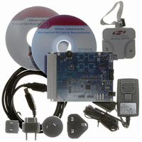
DEV KIT FOR C8051F700
Manufacturer
Silicon Laboratories Inc
Type
MCUr
Datasheets
1.C8051F700-TB.pdf
(1 pages)
2.C8051F700-TB.pdf
(306 pages)
3.C8051F700-TB.pdf
(18 pages)
Specifications of C8051F700DK
Contents
Board, Cables, CD, Debugger, Power Supply
Processor To Be Evaluated
C8051F7x
Processor Series
C8051F7xx
Interface Type
USB
Operating Supply Voltage
3.3 V
Lead Free Status / RoHS Status
Lead free / RoHS Compliant
For Use With/related Products
C8051F7xx
Lead Free Status / Rohs Status
Lead free / RoHS Compliant
Other names
336-1635


C8051F70x/71x
SFR Definition 15.10. CS0MD1: Capacitive Sense Mode 1
SFR Address = 0xAD; SFR Page = 0
94
Name
Reset
7:6
5:4
2:0
Bit
Type
3
Bit
CS0CG[2:0]
CS0DR[1:0]
Unused
Unused
Name
7
0
R
Read = 00b; Write = Don’t care
CS0 Double Reset Select.
These bits adjust the secondary CS0 reset time. For most touch-sensitive
switches, the default (fastest) value is sufficient, and these bits should not be
modified.
00: No additional time is used for secondary reset (recommended for most
switches)
01: An additional 0.75 µs is used for secondary reset.
10: An additional 1.5 µs is used for secondary reset.
11: An additional 2.25 µs is used for secondary reset.
Read = 0b; Write = Don’t care
CS0 Reference Gain Select.
These bits select the "gain" applied to the current used to charge an internal refer-
ence capacitor. Lower gain values decrease the current setting, and increase
both the size of the capacitance that can be measured with the CS0 module, and
the base conversion time. Refer to “15.2. CS0 Gain Adjustment” on page 81 for
more information.
000: Gain = 1x
001: Gain = 2x
010: Gain = 3x
011: Gain = 4x
100: Gain = 5x
101: Gain = 6x
110: Gain = 7x
111: Gain = 8x (default)
6
0
5
0
CS0DR[1:0]
R/W
Rev. 1.0
4
0
Description
R
3
0
R/W
2
1
CS0CG[2:0]
R/W
1
1
R/W
0
1
Related parts for C8051F700DK
Image
Part Number
Description
Manufacturer
Datasheet
Request
R

Part Number:
Description:
SMD/C°/SINGLE-ENDED OUTPUT SILICON OSCILLATOR
Manufacturer:
Silicon Laboratories Inc
Part Number:
Description:
Manufacturer:
Silicon Laboratories Inc
Datasheet:
Part Number:
Description:
N/A N/A/SI4010 AES KEYFOB DEMO WITH LCD RX
Manufacturer:
Silicon Laboratories Inc
Datasheet:
Part Number:
Description:
N/A N/A/SI4010 SIMPLIFIED KEY FOB DEMO WITH LED RX
Manufacturer:
Silicon Laboratories Inc
Datasheet:
Part Number:
Description:
N/A/-40 TO 85 OC/EZLINK MODULE; F930/4432 HIGH BAND (REV E/B1)
Manufacturer:
Silicon Laboratories Inc
Part Number:
Description:
EZLink Module; F930/4432 Low Band (rev e/B1)
Manufacturer:
Silicon Laboratories Inc
Part Number:
Description:
I°/4460 10 DBM RADIO TEST CARD 434 MHZ
Manufacturer:
Silicon Laboratories Inc
Part Number:
Description:
I°/4461 14 DBM RADIO TEST CARD 868 MHZ
Manufacturer:
Silicon Laboratories Inc
Part Number:
Description:
I°/4463 20 DBM RFSWITCH RADIO TEST CARD 460 MHZ
Manufacturer:
Silicon Laboratories Inc
Part Number:
Description:
I°/4463 20 DBM RADIO TEST CARD 868 MHZ
Manufacturer:
Silicon Laboratories Inc
Part Number:
Description:
I°/4463 27 DBM RADIO TEST CARD 868 MHZ
Manufacturer:
Silicon Laboratories Inc
Part Number:
Description:
I°/4463 SKYWORKS 30 DBM RADIO TEST CARD 915 MHZ
Manufacturer:
Silicon Laboratories Inc
Part Number:
Description:
N/A N/A/-40 TO 85 OC/4463 RFMD 30 DBM RADIO TEST CARD 915 MHZ
Manufacturer:
Silicon Laboratories Inc
Part Number:
Description:
I°/4463 20 DBM RADIO TEST CARD 169 MHZ
Manufacturer:
Silicon Laboratories Inc