C8051F700DK Silicon Laboratories Inc, C8051F700DK Datasheet - Page 4
C8051F700DK
Manufacturer Part Number
C8051F700DK
Description
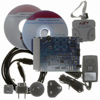
DEV KIT FOR C8051F700
Manufacturer
Silicon Laboratories Inc
Type
MCUr
Datasheets
1.C8051F700-TB.pdf
(1 pages)
2.C8051F700-TB.pdf
(306 pages)
3.C8051F700-TB.pdf
(18 pages)
Specifications of C8051F700DK
Contents
Board, Cables, CD, Debugger, Power Supply
Processor To Be Evaluated
C8051F7x
Processor Series
C8051F7xx
Interface Type
USB
Operating Supply Voltage
3.3 V
Lead Free Status / RoHS Status
Lead free / RoHS Compliant
For Use With/related Products
C8051F7xx
Lead Free Status / Rohs Status
Lead free / RoHS Compliant
Other names
336-1635


C8051F70x/71x
17. Memory Organization .......................................................................................... 108
18. External Data Memory Interface and On-Chip XRAM ....................................... 111
19. In-System Device Identification.......................................................................... 128
20. Special Function Registers................................................................................. 130
21. Interrupts .............................................................................................................. 137
22. Flash Memory....................................................................................................... 148
4
16.2. CIP-51 Register Descriptions ........................................................................ 104
17.1. Program Memory........................................................................................... 109
17.2. EEPROM Memory ......................................................................................... 109
17.3. Data Memory ................................................................................................. 109
18.1. Accessing XRAM........................................................................................... 111
18.2. Configuring the External Memory Interface ................................................... 112
18.3. Port Configuration.......................................................................................... 112
18.4. Multiplexed and Non-multiplexed Selection................................................... 115
18.5. Memory Mode Selection................................................................................ 117
18.6. Timing .......................................................................................................... 118
21.1. MCU Interrupt Sources and Vectors.............................................................. 138
21.2. Interrupt Register Descriptions ...................................................................... 140
21.3. INT0 and INT1 External Interrupts................................................................. 146
22.1. Programming The Flash Memory .................................................................. 148
16.1.1. Instruction and CPU Timing .................................................................... 99
17.1.1. MOVX Instruction and Program Memory .............................................. 109
17.3.1. Internal RAM ......................................................................................... 109
18.1.1. 16-Bit MOVX Example .......................................................................... 111
18.1.2. 8-Bit MOVX Example ............................................................................ 111
18.4.1. Multiplexed Configuration...................................................................... 115
18.4.2. Non-multiplexed Configuration.............................................................. 116
18.5.1. Internal XRAM Only .............................................................................. 117
18.5.2. Split Mode without Bank Select............................................................. 117
18.5.3. Split Mode with Bank Select.................................................................. 118
18.5.4. External Only......................................................................................... 118
18.6.1. Non-Multiplexed Mode .......................................................................... 120
18.6.2. Multiplexed Mode .................................................................................. 123
21.1.1. Interrupt Priorities.................................................................................. 138
21.1.2. Interrupt Latency ................................................................................... 138
22.1.1. Flash Lock and Key Functions .............................................................. 148
17.3.1.1. General Purpose Registers .......................................................... 110
17.3.1.2. Bit Addressable Locations ............................................................ 110
17.3.1.3. Stack .......................................................................................... 110
18.6.1.1. 16-bit MOVX: EMI0CF[4:2] = 101, 110, or 111............................. 120
18.6.1.2. 8-bit MOVX without Bank Select: EMI0CF[4:2] = 101 or 111 ....... 121
18.6.1.3. 8-bit MOVX with Bank Select: EMI0CF[4:2] = 110 ....................... 122
18.6.2.1. 16-bit MOVX: EMI0CF[4:2] = 001, 010, or 011............................. 123
18.6.2.2. 8-bit MOVX without Bank Select: EMI0CF[4:2] = 001 or 011 ....... 124
18.6.2.3. 8-bit MOVX with Bank Select: EMI0CF[4:2] = 010 ....................... 125
Rev. 1.0
Related parts for C8051F700DK
Image
Part Number
Description
Manufacturer
Datasheet
Request
R

Part Number:
Description:
SMD/C°/SINGLE-ENDED OUTPUT SILICON OSCILLATOR
Manufacturer:
Silicon Laboratories Inc
Part Number:
Description:
Manufacturer:
Silicon Laboratories Inc
Datasheet:
Part Number:
Description:
N/A N/A/SI4010 AES KEYFOB DEMO WITH LCD RX
Manufacturer:
Silicon Laboratories Inc
Datasheet:
Part Number:
Description:
N/A N/A/SI4010 SIMPLIFIED KEY FOB DEMO WITH LED RX
Manufacturer:
Silicon Laboratories Inc
Datasheet:
Part Number:
Description:
N/A/-40 TO 85 OC/EZLINK MODULE; F930/4432 HIGH BAND (REV E/B1)
Manufacturer:
Silicon Laboratories Inc
Part Number:
Description:
EZLink Module; F930/4432 Low Band (rev e/B1)
Manufacturer:
Silicon Laboratories Inc
Part Number:
Description:
I°/4460 10 DBM RADIO TEST CARD 434 MHZ
Manufacturer:
Silicon Laboratories Inc
Part Number:
Description:
I°/4461 14 DBM RADIO TEST CARD 868 MHZ
Manufacturer:
Silicon Laboratories Inc
Part Number:
Description:
I°/4463 20 DBM RFSWITCH RADIO TEST CARD 460 MHZ
Manufacturer:
Silicon Laboratories Inc
Part Number:
Description:
I°/4463 20 DBM RADIO TEST CARD 868 MHZ
Manufacturer:
Silicon Laboratories Inc
Part Number:
Description:
I°/4463 27 DBM RADIO TEST CARD 868 MHZ
Manufacturer:
Silicon Laboratories Inc
Part Number:
Description:
I°/4463 SKYWORKS 30 DBM RADIO TEST CARD 915 MHZ
Manufacturer:
Silicon Laboratories Inc
Part Number:
Description:
N/A N/A/-40 TO 85 OC/4463 RFMD 30 DBM RADIO TEST CARD 915 MHZ
Manufacturer:
Silicon Laboratories Inc
Part Number:
Description:
I°/4463 20 DBM RADIO TEST CARD 169 MHZ
Manufacturer:
Silicon Laboratories Inc