DEMO9S08JM16 Freescale Semiconductor, DEMO9S08JM16 Datasheet - Page 195
DEMO9S08JM16
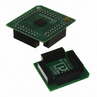
Manufacturer Part Number
DEMO9S08JM16
Description
BOARD DEMO FOR JM16 FAMI
Manufacturer
Freescale Semiconductor
Type
MCUr
Datasheets
1.DEMO9S08JM16.pdf
(47 pages)
2.DEMO9S08JM16.pdf
(5 pages)
3.DEMO9S08JM16.pdf
(4 pages)
4.DEMO9S08JM16.pdf
(386 pages)
Specifications of DEMO9S08JM16
Contents
Board with Daughter card, Cable, Documentation, Mini-AB USB Kit
Processor To Be Evaluated
MC9S08JM16
Data Bus Width
8 bit
Interface Type
USB
Silicon Manufacturer
Freescale
Core Architecture
HCS08
Core Sub-architecture
HCS08
Silicon Core Number
MC9S08
Silicon Family Name
Flexis - S08JM
Rohs Compliant
Yes
For Use With/related Products
MC9S08JM16
Lead Free Status / RoHS Status
Lead free / RoHS Compliant


To change from FEI clock mode to FBI clock mode, follow this procedure:
12.5.2
When switching between operational modes of the MCG, certain configuration bits must be changed in
order to properly move from one mode to another. Each time any of these bits are changed (PLLS, IREFS,
CLKS, or EREFS), the corresponding bits in the MCGSC register (PLLST, IREFST, CLKST, or
OSCINIT) must be checked before moving on in the application software.
Additionally, care must be taken to ensure that the reference clock divider (RDIV) is set properly for the
mode being switched to. For instance, in PEE mode, if using a 4 MHz crystal, RDIV must be set to %001
(divide-by-2) or %010 (divide-by-4) in order to divide the external reference down to the required
frequency between 1 and 2 MHz.
The RDIV and IREFS bits must always be set properly before changing the PLLS bit so that the FLL or
PLL clock has an appropriate reference clock frequency to switch to.
Freescale Semiconductor
3. After the proper configuration bits have been set, wait for the affected bits in the MCGSC register
1. Change the CLKS bits to %01 so that the internal reference clock is selected as the system clock
2. Wait for the CLKST bits in the MCGSC register to change to %01, indicating that the internal
to be changed appropriately, reflecting that the MCG has moved into the proper mode.
— If ERCLKEN was set in step 1 or the MCG is in FEE, FBE, PEE, PBE, or BLPE mode, and
— If in FEE mode, check to make sure the IREFST bit is cleared and the LOCK bit is set before
— If in FBE mode, check to make sure the IREFST bit is cleared, the LOCK bit is set, and the
source.
reference clock has been appropriately selected.
minimum power consumption, leave the internal reference disabled while in an external clock
mode.
EREFS was also set in step 1, wait here for the OSCINIT bit to become set indicating that the
external clock source has finished its initialization cycles and stabilized. Typical crystal startup
times are given in Appendix A, “Electrical Characteristics”.
moving on.
CLKST bits have changed to %10 indicating the external reference clock has been
appropriately selected. Although the FLL is bypassed in FBE mode, it is still on and will lock
in FBE mode.
MCG Mode Switching
MC9S08JM16 Series Data Sheet, Rev. 2
Multi-Purpose Clock Generator (S08MCGV1)
195
Related parts for DEMO9S08JM16
Image
Part Number
Description
Manufacturer
Datasheet
Request
R

Part Number:
Description:
Manufacturer:
Freescale Semiconductor, Inc
Datasheet:
Part Number:
Description:
Manufacturer:
Freescale Semiconductor, Inc
Datasheet:
Part Number:
Description:
Manufacturer:
Freescale Semiconductor, Inc
Datasheet:
Part Number:
Description:
Manufacturer:
Freescale Semiconductor, Inc
Datasheet:
Part Number:
Description:
Manufacturer:
Freescale Semiconductor, Inc
Datasheet:
Part Number:
Description:
Manufacturer:
Freescale Semiconductor, Inc
Datasheet:
Part Number:
Description:
Manufacturer:
Freescale Semiconductor, Inc
Datasheet:
Part Number:
Description:
Manufacturer:
Freescale Semiconductor, Inc
Datasheet:
Part Number:
Description:
Manufacturer:
Freescale Semiconductor, Inc
Datasheet:
Part Number:
Description:
Manufacturer:
Freescale Semiconductor, Inc
Datasheet:
Part Number:
Description:
Manufacturer:
Freescale Semiconductor, Inc
Datasheet:
Part Number:
Description:
Manufacturer:
Freescale Semiconductor, Inc
Datasheet:
Part Number:
Description:
Manufacturer:
Freescale Semiconductor, Inc
Datasheet:
Part Number:
Description:
Manufacturer:
Freescale Semiconductor, Inc
Datasheet:
Part Number:
Description:
Manufacturer:
Freescale Semiconductor, Inc
Datasheet: