DEMO9S08JM16 Freescale Semiconductor, DEMO9S08JM16 Datasheet - Page 48
DEMO9S08JM16
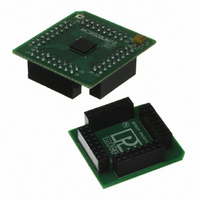
Manufacturer Part Number
DEMO9S08JM16
Description
BOARD DEMO FOR JM16 FAMI
Manufacturer
Freescale Semiconductor
Type
MCUr
Datasheets
1.DEMO9S08JM16.pdf
(47 pages)
2.DEMO9S08JM16.pdf
(5 pages)
3.DEMO9S08JM16.pdf
(4 pages)
4.DEMO9S08JM16.pdf
(386 pages)
Specifications of DEMO9S08JM16
Contents
Board with Daughter card, Cable, Documentation, Mini-AB USB Kit
Processor To Be Evaluated
MC9S08JM16
Data Bus Width
8 bit
Interface Type
USB
Silicon Manufacturer
Freescale
Core Architecture
HCS08
Core Sub-architecture
HCS08
Silicon Core Number
MC9S08
Silicon Family Name
Flexis - S08JM
Rohs Compliant
Yes
For Use With/related Products
MC9S08JM16
Lead Free Status / RoHS Status
Lead free / RoHS Compliant


Chapter 4 Memory
and erase pulses. An integer number of these timing pulses are used by the command processor to complete
a program or erase command.
Table 4-5
of FCLK (f
of cycles of FCLK and as an absolute time for the case where t
shown include overhead for the command state machine and enabling and disabling of program and erase
voltages.
4.5.3
The steps for executing any of the commands are listed below. The FCDIV register must be initialized and
any error flags cleared before beginning command execution. The command execution steps are:
A partial command sequence can be aborted manually by writing a 0 to FCBEF any time after the write to
the memory array and before writing the 1 that clears FCBEF and launches the complete command.
48
1. Write a data value to an address in the flash array. The address and data information from this write
2. Write the command code for the desired command to FCMD. The five valid commands are blank
3. Write a 1 to the FCBEF bit in FSTAT to clear FCBEF and launch the command (including its
is latched into the flash interface. This write is a required first step in any command sequence. For
erase and blank check commands, the value of the data is not important. For page erase commands,
the address may be any address in the 512-byte page of flash to be erased. For mass erase and blank
check commands, the address can be any address in the flash memory. Whole pages of 512 bytes
are the smallest block of flash that may be erased. In the 60K version, there are two instances where
the size of a block that is accessible to the user is less than 512 bytes: the first page following RAM,
and the first page following the high page registers. These pages are overlapped by the RAM and
high page registers respectively.
check (0x05), byte program (0x20), burst program (0x25), page erase (0x40), and mass erase
(0x41). The command code is latched into the command buffer.
address and data information).
shows program and erase times. The bus clock frequency and FCDIV determine the frequency
FCLK
Program and Erase Command Execution
1
Byte program
Byte program (burst)
Page erase
Mass erase
Do not program any byte in the flash more than once after a successful erase
operation. Reprogramming bits to a byte which is already programmed is
not allowed without first erasing the page in which the byte resides or mass
erasing the entire flash memory. Programming without first erasing may
disturb data stored in the flash.
Excluding start/end overhead
). The time for one cycle of FCLK is t
Parameter
Table 4-5. Program and Erase Times
MC9S08JM16 Series Data Sheet, Rev. 2
Cycles of FCLK
NOTE
20,000
4000
9
4
FCLK
= 1/f
FCLK
FCLK
Time if FCLK = 200 kHz
= 5 μs. Program and erase times
. The times are shown as a number
100 ms
20 μs
20 ms
45 μs
1
Freescale Semiconductor
Related parts for DEMO9S08JM16
Image
Part Number
Description
Manufacturer
Datasheet
Request
R

Part Number:
Description:
Manufacturer:
Freescale Semiconductor, Inc
Datasheet:
Part Number:
Description:
Manufacturer:
Freescale Semiconductor, Inc
Datasheet:
Part Number:
Description:
Manufacturer:
Freescale Semiconductor, Inc
Datasheet:
Part Number:
Description:
Manufacturer:
Freescale Semiconductor, Inc
Datasheet:
Part Number:
Description:
Manufacturer:
Freescale Semiconductor, Inc
Datasheet:
Part Number:
Description:
Manufacturer:
Freescale Semiconductor, Inc
Datasheet:
Part Number:
Description:
Manufacturer:
Freescale Semiconductor, Inc
Datasheet:
Part Number:
Description:
Manufacturer:
Freescale Semiconductor, Inc
Datasheet:
Part Number:
Description:
Manufacturer:
Freescale Semiconductor, Inc
Datasheet:
Part Number:
Description:
Manufacturer:
Freescale Semiconductor, Inc
Datasheet:
Part Number:
Description:
Manufacturer:
Freescale Semiconductor, Inc
Datasheet:
Part Number:
Description:
Manufacturer:
Freescale Semiconductor, Inc
Datasheet:
Part Number:
Description:
Manufacturer:
Freescale Semiconductor, Inc
Datasheet:
Part Number:
Description:
Manufacturer:
Freescale Semiconductor, Inc
Datasheet:
Part Number:
Description:
Manufacturer:
Freescale Semiconductor, Inc
Datasheet: