AD9549/PCBZ Analog Devices Inc, AD9549/PCBZ Datasheet - Page 34
AD9549/PCBZ
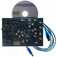
Manufacturer Part Number
AD9549/PCBZ
Description
BOARD EVALUATION FOR AD9549
Manufacturer
Analog Devices Inc
Datasheet
1.AD9549ABCPZ.pdf
(76 pages)
Specifications of AD9549/PCBZ
Main Purpose
Timing, Clock Generator
Embedded
No
Utilized Ic / Part
AD9549
Primary Attributes
2 Inputs, 2 Outputs, VCO
Secondary Attributes
CMOS, HSTL Output Logic, Graphical User Interface
Lead Free Status / RoHS Status
Lead free / RoHS Compliant


AD9549
The SYSCLK PLL multiplier path is enabled by a Logic 0
(default) in the PD SYSCLK PLL bit of the I/O register map.
The SYSCLK PLL multiplier can be driven from the SYSCLK
input pins by one of two means depending on the logic level
applied to the 1.8V CMOS CLKMODESEL pin. When
CLKMODESEL = 0, a crystal can be connected directly across
the SYSCLK pins. When CLKMODESEL = 1, the maintaining
amp is disabled, and an external frequency source (oscillator,
signal generator, etc.) can be connected directly to the SYSCLK
input pins. Note that CLKMODESEL = 1 does not disable the
system clock PLL.
The maintaining amp on the AD9549 SYSCLK pins is intended for
25 MHz, 3.2 mm × 2.5 mm AT cut fundamental mode crystals
with a maximum motional resistance of 100 Ω. The following
crystals, listed in alphabetical order, meet these criteria (as of
the revision date of this data sheet):
•
•
•
•
•
Note that while these crystals meet the preceding criteria
according to their data sheets, Analog Devices, Inc., does not
guarantee their operation with the AD9549, nor does Analog
Devices endorse one supplier of crystals over another.
When the SYSCLK PLL multiplier path is disabled, the AD9549
must be driven by a high frequency signal source (500 MHz to
1 GHz). The signal thus applied to the SYSCLK input pins
becomes the internal DAC sampling clock (f
through an internal buffer.
SYSCLK PLL Doubler
The SYSCLK PLL multiplier path offers an optional SYSCLK
PLL doubler. This block comes before the SYSCLK PLL
multiplier and acts as a frequency doubler by generating a pulse
on each edge of the SYSCLK input signal. The SYSCLK PLL
multiplier locks to the falling edges of this regenerated signal.
The impetus for doubling the frequency at the input of the
SYSCLK PLL multiplier is that an improvement in overall phase
noise performance can be realized. The main drawback is that
the doubler output is not a rectangular pulse with a constant
duty cycle even for a perfectly symmetric SYSCLK input signal.
This results in a subharmonic appearing at the same frequency
as the SYSCLK input signal, and the magnitude of the subhar-
monic can be quite large. When employing the doubler, care
must be taken to ensure that the loop bandwidth of the SYSCLK
PLL multiplier adequately suppresses the subharmonic.
AVX/Kyocera CX3225SB
ECS ECX-32
Epson/Toyocom TSX-3225
Fox FX3225BS
NDK NX3225SA
S
) after passing
Rev. D | Page 34 of 76
The benefit offered by the doubler depends on the magnitude
of the subharmonic, the loop bandwidth of the SYSCLK PLL
multiplier, and the overall phase noise requirements of the
specific application. In many applications, the AD9549 clock
output is applied to the input of another PLL, and the
subharmonic is often suppressed by the relatively narrow
bandwidth of the downstream PLL.
Note that generally, the benefits of the SYSCLK PLL doubler are
realized for SYSCLK input frequencies of 25 MHz and above.
SYSCLK PLL Multiplier
When the SYSCLK PLL multiplier path is employed, the
frequency applied to the SYSCLK input pins must be limited so
as not to exceed the maximum input frequency of the SYSCLK
PLL phase detector. A block diagram of the SYSCLK generator
is shown in Figure 43.
The SYSCLK PLL multiplier has a 1 GHz VCO at its core. A phase/
frequency detector (PFD) and charge pump provide the steering
signal to the VCO in typical PLL fashion. The PFD operates on
the falling edge transitions of the input signal, which means that
the loop locks on the negative edges of the reference signal. The
charge pump gain is controlled via the I/O register map by selecting
one of three possible constant current sources ranging from 125 μA
to 375 μA in 125 μA steps. The center frequency of the VCO is
also adjustable via the I/O register map and provides high/low
gain selection. The feedback path from VCO to PFD consists of
a fixed divide-by-2 prescaler followed by a programmable divide-
by-N block, where 2 ≤ N ≤ 33. This limits the overall divider
range to any even integer from 4 to 66, inclusive. The value of
N is programmed via the I/O register map via a 5-bit word that
spans a range of 0 to 31, but the internal logic automatically adds
a bias of 2 to the value entered, extending the range to 33. Care
should be taken when choosing these values so as to not exceed
the maximum input frequency of the SYSCLK PLL phase detector
or SYSCLK PLL doubler. These values can be found in the AC
Specifications section.
SYSCLK
FROM
INPUT
FREQUENCY
DETECTOR
Figure 43. Block Diagram of the SYSCLK PLL
PHASE
SYSCLK PLL MULTIPLIER
(125µA, 250µA, 375µA)
~2pF
LOOP_FILTER
CHARGE
PUMP
2
I
CP
(N = 2 TO 33)
÷N
(HI/LO)
1GHz
K
VCO
÷2
VCO
DAC
SAMPLE
CLOCK
Related parts for AD9549/PCBZ
Image
Part Number
Description
Manufacturer
Datasheet
Request
R


Part Number:
Description:
±1.7g Dual-Axis IMEMS Accelerometer Evaluation Board
Manufacturer:
Analog Devices Inc
Datasheet:

Part Number:
Description:
Inertial Sensor Evaluation System
Manufacturer:
Analog Devices Inc
Datasheet:
Part Number:
Description:
Manufacturer:
Analog Devices Inc
Datasheet:
Part Number:
Description:
Manufacturer:
Analog Devices Inc
Datasheet:
Part Number:
Description:
Manufacturer:
Analog Devices Inc
Datasheet:
Part Number:
Description:
Manufacturer:
Analog Devices Inc
Datasheet:
Part Number:
Description:
Manufacturer:
Analog Devices Inc
Datasheet:
Part Number:
Description:
Manufacturer:
Analog Devices Inc
Datasheet:
Part Number:
Description:
Manufacturer:
Analog Devices Inc
Datasheet:
Part Number:
Description:
Manufacturer:
Analog Devices Inc
Datasheet:
Part Number:
Description:
Manufacturer:
Analog Devices Inc
Datasheet:
Part Number:
Description:
Manufacturer:
Analog Devices Inc
Datasheet: