AD9549/PCBZ Analog Devices Inc, AD9549/PCBZ Datasheet - Page 9
AD9549/PCBZ
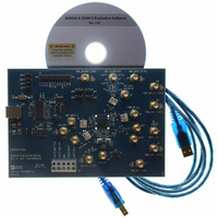
Manufacturer Part Number
AD9549/PCBZ
Description
BOARD EVALUATION FOR AD9549
Manufacturer
Analog Devices Inc
Datasheet
1.AD9549ABCPZ.pdf
(76 pages)
Specifications of AD9549/PCBZ
Main Purpose
Timing, Clock Generator
Embedded
No
Utilized Ic / Part
AD9549
Primary Attributes
2 Inputs, 2 Outputs, VCO
Secondary Attributes
CMOS, HSTL Output Logic, Graphical User Interface
Lead Free Status / RoHS Status
Lead free / RoHS Compliant


ABSOLUTE MAXIMUM RATINGS
Table 3.
Parameter
Analog Supply Voltage (AVDD)
Digital Supply Voltage (DVDD)
Digital I/O Supply Voltage
DAC Supply Voltage (AVDD3 Pins)
Maximum Digital Input Voltage
Storage Temperature
Operating Temperature Range
Lead Temperature
Junction Temperature
Stresses above those listed under Absolute Maximum Ratings
may cause permanent damage to the device. This is a stress
rating only; functional operation of the device at these or any
other conditions above those indicated in the operational
section of this specification is not implied. Exposure to absolute
maximum rating conditions for extended periods may affect
device reliability.
(DVDD_I/O)
(Soldering, 10 sec)
300°C
Rating
2 V
2 V
3.6 V
3.6 V
−0.5 V to DVDD_I/O + 0.5 V
−65°C to +150°C
−40°C to +85°C
150°C
Rev. D | Page 9 of 76
THERMAL RESISTANCE
θ
soldered in a circuit board for surface-mount packages.
Table 4. Thermal Resistance
Package Type
64-Lead LFCSP
Note that the exposed pad on the bottom of the package must
be soldered to ground to achieve the specified thermal perfor-
mance. See the Thermal Performance section for more
information.
ESD CAUTION
JA
is specified for the worst-case conditions, that is, a device
θ
25.2
JA
θ
13.9
JB
θ
1.7
JC
Unit
°C/W typical
AD9549
Related parts for AD9549/PCBZ
Image
Part Number
Description
Manufacturer
Datasheet
Request
R


Part Number:
Description:
±1.7g Dual-Axis IMEMS Accelerometer Evaluation Board
Manufacturer:
Analog Devices Inc
Datasheet:

Part Number:
Description:
Inertial Sensor Evaluation System
Manufacturer:
Analog Devices Inc
Datasheet:
Part Number:
Description:
Manufacturer:
Analog Devices Inc
Datasheet:
Part Number:
Description:
Manufacturer:
Analog Devices Inc
Datasheet:
Part Number:
Description:
Manufacturer:
Analog Devices Inc
Datasheet:
Part Number:
Description:
Manufacturer:
Analog Devices Inc
Datasheet:
Part Number:
Description:
Manufacturer:
Analog Devices Inc
Datasheet:
Part Number:
Description:
Manufacturer:
Analog Devices Inc
Datasheet:
Part Number:
Description:
Manufacturer:
Analog Devices Inc
Datasheet:
Part Number:
Description:
Manufacturer:
Analog Devices Inc
Datasheet:
Part Number:
Description:
Manufacturer:
Analog Devices Inc
Datasheet:
Part Number:
Description:
Manufacturer:
Analog Devices Inc
Datasheet: