AD9549/PCBZ Analog Devices Inc, AD9549/PCBZ Datasheet - Page 43
AD9549/PCBZ
Manufacturer Part Number
AD9549/PCBZ
Description
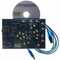
BOARD EVALUATION FOR AD9549
Manufacturer
Analog Devices Inc
Datasheet
1.AD9549ABCPZ.pdf
(76 pages)
Specifications of AD9549/PCBZ
Main Purpose
Timing, Clock Generator
Embedded
No
Utilized Ic / Part
AD9549
Primary Attributes
2 Inputs, 2 Outputs, VCO
Secondary Attributes
CMOS, HSTL Output Logic, Graphical User Interface
Lead Free Status / RoHS Status
Lead free / RoHS Compliant


POWER SUPPLY PARTITIONING
The AD9549 features multiple power supplies, and their power
consumption varies with its configuration. This section covers
which power supplies can be grouped together and how the
consumption of each power block varies with frequency.
The numbers quoted here are for comparison only. Refer to the
Specifications section for exact numbers. With each group, use
bypass capacitors of 1 μF in parallel with a 10 μF.
The recommendations here are for typical applications, and for
these applications, there are four groups of power supplies:
3.3 V digital, 3.3 V analog, 1.8 V digital, and 1.8 V analog.
Applications demanding the highest performance may require
additional power supply isolation.
Note that all power supply pins must receive power regardless of
whether that block is used.
3.3 V SUPPLIES
DVDD_I/O (Pin 1) and AVDD3 (Pin 14)
Although one of these pins is analog and the other is digital,
these two 3.3 V supplies can be grouped together. The power
consumption on Pin 1 varies dynamically with serial port activity.
AVDD3 (Pin 37)
Pin 37 is the CMOS driver supply. It can be either 1.8 V or 3.3 V,
and its power consumption is a function of the output frequency
and loading of OUT_CMOS (Pin 38).
If the CMOS driver is used at 3.3 V, this supply should be isolated
from other 3.3 V supplies with a ferrite bead to avoid a spur at
the output frequency. If the HSTL driver is not used, AVDD3
(Pin 37) can be connected (using a ferrite bead) to AVDD3
(Pin 46, Pin 47, Pin 49). If the HSTL driver is used, connect
AVDD3 (Pin 37) to Pin 1 and Pin 14, using a ferrite bead.
If the CMOS driver is used at 1.8 V, AVDD3 (Pin 37) can be
connected to AVDD (Pin 36).
If the CMOS driver is not used, AVDD3 (Pin 37) can be tied
directly to the 1.8 V AVDD (Pin 36) and the CMOS driver
powered down using Register 0x0010.
AVDD3 (Pin 46, Pin 47, Pin 49)
These are 3.3 V DAC power supplies that typically consume
about 25 mA. At a minimum, a ferrite bead should be used to
isolate these from other 3.3 V supplies, with a separate regulator
being ideal.
Rev. D | Page 43 of 76
1.8 V SUPPLIES
DVDD (Pin 3, Pin 5, Pin 7)
These pins should be grouped together and isolated from the
1.8 V AVDD supplies. For most applications, a ferrite bead
provides sufficient isolation, but a separate regulator may be
necessary for applications demanding the highest performance.
The current consumption of this group increases from about
160 mA at a system clock of 700 MHz to about 205 mA at a
system clock of 1 GHz. There is also a slight (~5%) increase as
f
AVDD (Pin 11, Pin 19, Pin 23, Pin 24, Pin 36, Pin 42, Pin 44,
and Pin 45)
These pins can be grouped together and should be isolated from
other 1.8 V supplies. A separate regulator is recommended. At a
minimum, a ferrite bead should be used for isolation.
AVDD (Pin 53)
This 1.8 V supply consumes about 40 mA. The supply can be
run off the same regulator as 1.8 V AVDD group, with a ferrite
bead to isolate Pin 53 from the rest of the 1.8 V AVDD group.
However, for applications demanding the highest performance,
a separate regulator is recommended.
AVDD (Pin 25, Pin 26, Pin 29, Pin 30)
These system clock PLL power pins should be grouped together
and isolated from other 1.8 V AVDD supplies.
At a minimum, it is recommended that Pin 25 and Pin 30 be
tied together and isolated from the aggregate AVDD 1.8 V supply
with a ferrite bead. Likewise, Pin 26 and Pin 29 can also be tied
together, with a ferrite bead isolating them from the same aggregate
1.8 V supply. The loop filter for the system clock PLL should
directly connect to Pin 26 and Pin 29 (see Figure 44).
Applications demanding the highest performance may require
that these four pins be powered by their own LDO.
If the system clock PLL is bypassed, the loop filter pin (Pin 31)
should be pulled down to analog ground using a 1 kΩ resistor.
Pin 25, Pin 26, Pin 29, and Pin 30 should be included in the large
1.8 V AVDD power supply group. In this mode, isolation of these
pins is not critical, and these pins consume almost no power.
OUT
increases from 50 MHz to 400 MHz.
AD9549
Related parts for AD9549/PCBZ
Image
Part Number
Description
Manufacturer
Datasheet
Request
R


Part Number:
Description:
±1.7g Dual-Axis IMEMS Accelerometer Evaluation Board
Manufacturer:
Analog Devices Inc
Datasheet:

Part Number:
Description:
Inertial Sensor Evaluation System
Manufacturer:
Analog Devices Inc
Datasheet:
Part Number:
Description:
Manufacturer:
Analog Devices Inc
Datasheet:
Part Number:
Description:
Manufacturer:
Analog Devices Inc
Datasheet:
Part Number:
Description:
Manufacturer:
Analog Devices Inc
Datasheet:
Part Number:
Description:
Manufacturer:
Analog Devices Inc
Datasheet:
Part Number:
Description:
Manufacturer:
Analog Devices Inc
Datasheet:
Part Number:
Description:
Manufacturer:
Analog Devices Inc
Datasheet:
Part Number:
Description:
Manufacturer:
Analog Devices Inc
Datasheet:
Part Number:
Description:
Manufacturer:
Analog Devices Inc
Datasheet:
Part Number:
Description:
Manufacturer:
Analog Devices Inc
Datasheet:
Part Number:
Description:
Manufacturer:
Analog Devices Inc
Datasheet: