AD9549/PCBZ Analog Devices Inc, AD9549/PCBZ Datasheet - Page 6
AD9549/PCBZ
Manufacturer Part Number
AD9549/PCBZ
Description
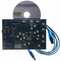
BOARD EVALUATION FOR AD9549
Manufacturer
Analog Devices Inc
Datasheet
1.AD9549ABCPZ.pdf
(76 pages)
Specifications of AD9549/PCBZ
Main Purpose
Timing, Clock Generator
Embedded
No
Utilized Ic / Part
AD9549
Primary Attributes
2 Inputs, 2 Outputs, VCO
Secondary Attributes
CMOS, HSTL Output Logic, Graphical User Interface
Lead Free Status / RoHS Status
Lead free / RoHS Compliant


AD9549
AC SPECIFICATIONS
f
Table 2.
Parameter
REFERENCE INPUTS
FDBK_IN INPUT
SYSTEM CLOCK INPUT
CLOCK DRIVERS
S
= 1 GHz, DAC R
Frequency Range (Sine Wave)
Frequency Range (CMOS)
Frequency Range (LVPECL)
Frequency Range (LVDS)
Minimum Slew Rate
Minimum Pulse Width High
Minimum Pulse Width Low
Input Frequency Range
Minimum Differential Input Level
Minimum Slew Rate
SYSCLK PLL Bypassed
SYSCLK PLL Enabled
Crystal Resonator with SYSCLK PLL Enabled
HSTL Output Driver
HSTL Output Driver with 2× Multiplier
Input Frequency Range
Duty Cycle
Minimum Differential Input Level
VCO Frequency Range, Low Band
VCO Frequency Range, Auto Band
VCO Frequency Range, High Band
Maximum Input Rate of System Clock PFD
Without SYSCLK PLL Doubler
With SYSCLK PLL Doubler
Crystal Resonator Frequency Range
Maximum Crystal Motional Resistance
Frequency Range
Duty Cycle
Rise Time/Fall Time (20-80%)
Jitter (12 kHz to 20 MHz)
Frequency Range
Duty Cycle
Rise Time/Fall Time (20% to 80%)
Subharmonic Spur Level
Jitter (12 kHz to 20 MHz)
Input Frequency Range
Multiplication Range
Minimum Differential Input Level
Input Frequency Range
Multiplication Range
Input Duty Cycle
Minimum Differential Input Level
SET
= 10 kΩ, power supply pins within the range specified in the DC Specifications section, unless otherwise noted.
Min
10
0.008
0.008
0.008
0.04
620
620
10
225
40
250
45
632
700
810
900
11
4
632
6
8
632
10
20
48
400
45
Typ
50
115
1.0
115
−35
1.1
Rev. D | Page 6 of 76
Max
750
50
725
725
400
1000
55
810
900
1000
200
200
66
100
132
50
100
725
52
165
725
55
165
Unit
MHz
MHz
MHz
MHz
V/ns
ps
ps
MHz
mV p-p
V/μs
MHz
%
mV p-p
MHz
MHz
MHz
MHz
MHz
mV p-p
MHz
%
mV p-p
MHz
Ω
MHz
%
ps
ps
MHz
%
ps
dBc
ps
Test Conditions/Comments
Pin 12, Pin 13, Pin 15, and Pin 16
Minimum recommended slew rate: 40 V/μs
LVDS must be ac-coupled; lower frequency bound may
be higher, depending on the size of the decoupling
capacitor
Pin 40, Pin 41
−12 dBm into 50 Ω; must be ac-coupled
Pin 27, Pin 28
Maximum f
0 dBm into 50 Ω
When in the range, use the low VCO band exclusively
When in the range, use the VCO Auto band select
When in the range, use the high VCO band exclusively
Integer multiples of 2, maximum PFD rate and system
clock frequency must be met
0 dBm into 50 Ω
Integer multiples of 8
Deviating from 50% duty cycle may adversely affect
spurious performance.
0 dBm into 50 Ω
AT cut, fundamental mode resonator
See the
See
100 Ω termination across OUT/OUTB, 2 pF load
f
clock input (see
100 Ω termination across OUT/OUTB, 2 pF load
Without correction
f
clock input (see
IN
IN
= 19.44 MHz, f
= 19.44 MHz, f
Figure 12
SYSCLK Inputs
OUT
is 0.4 × f
for maximum toggle rate
Figure 3
Figure 3
OUT
OUT
= 155.52 MHz. 50 MHz system
= 622.08 MHz, 50 MHz system
SYSCLK
section for recommendations
to
to
Figure 11
Figure 11
for test conditions)
for test conditions)
Related parts for AD9549/PCBZ
Image
Part Number
Description
Manufacturer
Datasheet
Request
R


Part Number:
Description:
±1.7g Dual-Axis IMEMS Accelerometer Evaluation Board
Manufacturer:
Analog Devices Inc
Datasheet:

Part Number:
Description:
Inertial Sensor Evaluation System
Manufacturer:
Analog Devices Inc
Datasheet:
Part Number:
Description:
Manufacturer:
Analog Devices Inc
Datasheet:
Part Number:
Description:
Manufacturer:
Analog Devices Inc
Datasheet:
Part Number:
Description:
Manufacturer:
Analog Devices Inc
Datasheet:
Part Number:
Description:
Manufacturer:
Analog Devices Inc
Datasheet:
Part Number:
Description:
Manufacturer:
Analog Devices Inc
Datasheet:
Part Number:
Description:
Manufacturer:
Analog Devices Inc
Datasheet:
Part Number:
Description:
Manufacturer:
Analog Devices Inc
Datasheet:
Part Number:
Description:
Manufacturer:
Analog Devices Inc
Datasheet:
Part Number:
Description:
Manufacturer:
Analog Devices Inc
Datasheet:
Part Number:
Description:
Manufacturer:
Analog Devices Inc
Datasheet: