AD9549/PCBZ Analog Devices Inc, AD9549/PCBZ Datasheet - Page 62
AD9549/PCBZ
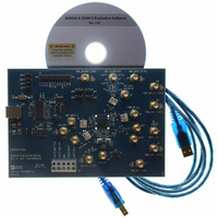
Manufacturer Part Number
AD9549/PCBZ
Description
BOARD EVALUATION FOR AD9549
Manufacturer
Analog Devices Inc
Datasheet
1.AD9549ABCPZ.pdf
(76 pages)
Specifications of AD9549/PCBZ
Main Purpose
Timing, Clock Generator
Embedded
No
Utilized Ic / Part
AD9549
Primary Attributes
2 Inputs, 2 Outputs, VCO
Secondary Attributes
CMOS, HSTL Output Logic, Graphical User Interface
Lead Free Status / RoHS Status
Lead free / RoHS Compliant


AD9549
Register 0x01AC to Register 0x01AD—Phase
Table 66.
Bits
[7:0]
Register 0x01AD—Phase (Continued)
Table 67.
Bits
[15:8]
REFERENCE SELECTOR/HOLDOVER (REGISTER 0x01C0 TO REGISTER 0x01C3)
Register 0x01C0—Automatic Control
Table 68.
Bits
4
3
2
1
0
Register 0x01C1—Override
Table 69.
Bits
4
3
2
1
0
Register 0x01C2—Averaging Window
Table 70.
Bits
[3:0]
Bit Name
DDS phase word
Bit Name
DDS phase word
Bit Name
Holdover mode
Reserved
Automatic selector
Automatic recover
Automatic holdover
Bit Name
Enable line card mode
Enable ref input
override
REF_AB
Enable holdover
override
Holdover on/off
Bit Name
FTW windowed
average size
Description
Allows user to vary the phase of the DDS output. See the Direct Digital Synthesizer section. Register
0x01AC is the least significant byte of the phase offset word (POW). Note that a momentary phase
discontinuity may occur as the phase passes through 45° intervals. Active only when the loop is not closed.
Description
This bit determines which frequency tuning word (FTW) is used in holdover mode.
0 = use last FTW at time of holdover.
1 = use averaged FTW at time of holdover, which is the recommended setting. The number of averages
used is set in Register 0x01C2.
Reserved.
Setting this bit permits state machine to switch the active reference clock input.
Setting this bit permits state machine to leave holdover mode.
Setting this bit permits state machine to enter holdover (free-run) mode.
Description
Enables line card mode of reference switch MUX, which eliminates the possibility of a runt pulse during
switchover. See the Use of Line Card Mode to Eliminate Runt Pulses section.
Setting this bit disables automatic reference switchover, and allows user to switch references manually
via Bit 2 of this register. Setting this bit overrides the REFSELECT pin.
This bit selects the input when Bit 3 of this register is set.
0 = REFA.
Setting this bit disables automatic holdover and allows user to enter/exit holdover manually via Bit 0
(see the description for Bit 0). Setting this bit overrides the HOLDOVER pin.
This bit controls the status of holdover when Bit 1 of this register is set.
Description
This register sets the number of FTWs (frequency tuning words) that are used for calculating the average
FTW. Bit 4 in Register 0x01C0 enables this feature. An average size of at least 32,000 is recommended for
most applications. The number of averages equals 2
the rate of (fs/2
PIO
).
Rev. D | Page 62 of 76
(FTW Windowed Average Size [3:0])
. These samples are taken at
Related parts for AD9549/PCBZ
Image
Part Number
Description
Manufacturer
Datasheet
Request
R


Part Number:
Description:
±1.7g Dual-Axis IMEMS Accelerometer Evaluation Board
Manufacturer:
Analog Devices Inc
Datasheet:

Part Number:
Description:
Inertial Sensor Evaluation System
Manufacturer:
Analog Devices Inc
Datasheet:
Part Number:
Description:
Manufacturer:
Analog Devices Inc
Datasheet:
Part Number:
Description:
Manufacturer:
Analog Devices Inc
Datasheet:
Part Number:
Description:
Manufacturer:
Analog Devices Inc
Datasheet:
Part Number:
Description:
Manufacturer:
Analog Devices Inc
Datasheet:
Part Number:
Description:
Manufacturer:
Analog Devices Inc
Datasheet:
Part Number:
Description:
Manufacturer:
Analog Devices Inc
Datasheet:
Part Number:
Description:
Manufacturer:
Analog Devices Inc
Datasheet:
Part Number:
Description:
Manufacturer:
Analog Devices Inc
Datasheet:
Part Number:
Description:
Manufacturer:
Analog Devices Inc
Datasheet:
Part Number:
Description:
Manufacturer:
Analog Devices Inc
Datasheet: