AD9549/PCBZ Analog Devices Inc, AD9549/PCBZ Datasheet - Page 4
AD9549/PCBZ
Manufacturer Part Number
AD9549/PCBZ
Description
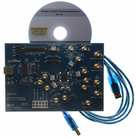
BOARD EVALUATION FOR AD9549
Manufacturer
Analog Devices Inc
Datasheet
1.AD9549ABCPZ.pdf
(76 pages)
Specifications of AD9549/PCBZ
Main Purpose
Timing, Clock Generator
Embedded
No
Utilized Ic / Part
AD9549
Primary Attributes
2 Inputs, 2 Outputs, VCO
Secondary Attributes
CMOS, HSTL Output Logic, Graphical User Interface
Lead Free Status / RoHS Status
Lead free / RoHS Compliant


AD9549
SPECIFICATIONS
DC SPECIFICATIONS
AVDD = 1.8 V ± 5%, AVDD3 = 3.3 V ± 5%, DVDD = 1.8 V ± 5%, DVDD_I/O = 3.3 V ± 5%. AVSS = 0 V, DVSS = 0 V, unless otherwise noted.
Table 1.
Parameter
SUPPLY VOLTAGE
SUPPLY CURRENT
LOGIC INPUTS (Except Pin 32)
CLKMODESEL (Pin 32) LOGIC INPUT
LOGIC OUTPUTS
REFERENCE INPUTS
FDBK_IN INPUT
DVDD_I/O (Pin 1)
DVDD (Pin 3, Pin 5, Pin 7)
AVDD3 (Pin 14, Pin 46, Pin 47, Pin 49)
AVDD3 (Pin 37)
AVDD (Pin 11, Pin 19, Pin 23 to Pin 26, Pin 29,
I
I
I
I
I
I
I
I
I
Input High Voltage (V
Input Low Voltage (V
Input Current (I
Maximum Input Capacitance (C
Input High Voltage (V
Input Low Voltage (V
Input Current (I
Maximum Input Capacitance (C
Output High Voltage (V
Output Low Voltage (V
Input Capacitance
Input Resistance
Differential Operation
Single-Ended Operation
Input Capacitance
Input Resistance
Differential Input Voltage Swing
AVDD3
AVDD3
AVDD3
AVDD
AVDD
AVDD
AVDD
DVDD
DVDD_I/O
Pin 30, Pin 36, Pin 42, Pin 44, Pin 45, Pin 53)
Pin 30, Pin 44, Pin 45)
Common Mode Input Voltage
Differential Input Voltage Swing
Input Voltage High (V
Input Voltage Low (V
Threshold Voltage
Input Current
(Pin 36, Pin 42)
(Pin 11)
(Pin 19, Pin 23 to Pin 26, Pin 29,
(Pin 53)
(Pin 3, Pin 5, Pin 7)
(Pin 14)
(Pin 37)
(Pin 46, Pin 47, Pin 49)
(Applicable When DC-Coupled)
(Pin 1)
INH
INH
, I
, I
INL
INL
IL
IL
)
)
IH
IH
)
)
)
)
OL
OH
IL
IH
)
)
)
)
IN
IN
2
)
)
1
1
Min
3.135
1.71
3.135
1.71
1.71
2.0
DVSS
1.4
AVSS
2.7
DVSS
8.5
1.5
500
2.0
AVSS
AVDD3 −
0.66
18
225
Typ
3.30
1.80
3.30
3.30
1.80
4.7
3.8
26
21
12
215
41
254
4
±60
3
−18
3
3
11.5
AVDD3 −
0.82
3
22
Rev. D | Page 4 of 76
Max
3.465
1.89
3.465
3.465
1.89
5.6
4.5
29
26
15
281
49
265
6
DVDD_I/O
0.8
±200
AVDD
0.4
−50
DVDD_I/O
0.4
14.5
AVDD3 −
0.2
AVDD3
0.8
AVDD3 −
0.98
1
26
Unit
V
V
V
V
V
mA
mA
mA
mA
mA
mA
mA
mA
mA
V
V
µA
pF
V
V
µA
pF
V
V
pF
kΩ
V
mV p-p
V
V
V
mA
pF
kΩ
mV p-p
Test Conditions/Comments
Pin 37 is typically 3.3 V, but can be set to 1.8 V
REFA, REFB buffers
CMOS output clock driver at 3.3 V
DAC output current source, f
FDBK_IN input, HSTL output clock driver
(output doubler turned on)
REFA and REFB input buffer 1.8 V supply
Aggregate analog supply, including system
clock PLL
DAC power supply
Digital core
Digital I/O (varies dynamically)
Pin 9, Pin 10, Pin 54 to Pin 61, Pin 63, Pin 64
At V
Pin 32 only
At V
Pin 62 and the following bidirectional pins:
Pin 9, Pin 10, Pin 54, Pin 55, Pin 63
I
I
Pin 12, Pin 13, Pin 15, Pin 16
Differential at Register 0x040F[1:0] = 00
Differential operation; note that LVDS signals
must be ac-coupled
Differential operation
Register 0x040F[1:0] = 10
Register 0x040F[1:0] = 10 (other settings
possible)
Single-ended operation
Pin 40, Pin 41
Differential
−12 dBm into 50 Ω; must be ac-coupled
OH
OL
= 1 mA
= 1 mA
IN
IN
= 0 V and V
= 0 V and V
IN
IN
= DVDD_I/O
= AVDD
S
= 1 GSPS
Related parts for AD9549/PCBZ
Image
Part Number
Description
Manufacturer
Datasheet
Request
R


Part Number:
Description:
±1.7g Dual-Axis IMEMS Accelerometer Evaluation Board
Manufacturer:
Analog Devices Inc
Datasheet:

Part Number:
Description:
Inertial Sensor Evaluation System
Manufacturer:
Analog Devices Inc
Datasheet:
Part Number:
Description:
Manufacturer:
Analog Devices Inc
Datasheet:
Part Number:
Description:
Manufacturer:
Analog Devices Inc
Datasheet:
Part Number:
Description:
Manufacturer:
Analog Devices Inc
Datasheet:
Part Number:
Description:
Manufacturer:
Analog Devices Inc
Datasheet:
Part Number:
Description:
Manufacturer:
Analog Devices Inc
Datasheet:
Part Number:
Description:
Manufacturer:
Analog Devices Inc
Datasheet:
Part Number:
Description:
Manufacturer:
Analog Devices Inc
Datasheet:
Part Number:
Description:
Manufacturer:
Analog Devices Inc
Datasheet:
Part Number:
Description:
Manufacturer:
Analog Devices Inc
Datasheet:
Part Number:
Description:
Manufacturer:
Analog Devices Inc
Datasheet: