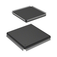
HD6417727F160V Renesas Electronics America, HD6417727F160V Datasheet - Page 10

HD6417727F160V
Manufacturer Part Number
HD6417727F160V
Description
MPU 3V 16K PB-FREE 240-QFP
Manufacturer
Renesas Electronics America
Series
SuperH® SH7700r
Datasheet
1.HD6417727BP100CV.pdf
(1098 pages)
Specifications of HD6417727F160V
Core Processor
SH-3 DSP
Core Size
32-Bit
Speed
160MHz
Connectivity
FIFO, SCI, SIO, SmartCard, USB
Peripherals
DMA, LCD, POR, WDT
Number Of I /o
104
Program Memory Type
ROMless
Ram Size
32K x 8
Voltage - Supply (vcc/vdd)
1.7 V ~ 2.05 V
Data Converters
A/D 6x10b; D/A 2x8b
Oscillator Type
Internal
Operating Temperature
-20°C ~ 75°C
Package / Case
240-QFP
Lead Free Status / RoHS Status
Lead free / RoHS Compliant
Eeprom Size
-
Program Memory Size
-
Available stocks
Company
Part Number
Manufacturer
Quantity
Price
Company:
Part Number:
HD6417727F160V
Manufacturer:
HITACHI
Quantity:
9
Company:
Part Number:
HD6417727F160V
Manufacturer:
Renesas Electronics America
Quantity:
10 000
Part Number:
HD6417727F160V
Manufacturer:
RENESAS/瑞萨
Quantity:
20 000
- Current page: 10 of 1098
- Download datasheet (7Mb)
Rev.6.00 Mar. 27, 2009 Page viii of lvi
REJ09B0254-0600
Page
323
331
332
333
336
337
338
339
12.3.2 Description of Areas
Area 2:
When synchronous DRAM is connected,
the RAS3 signal, CAS signal, RD/WR
signal, and byte controls DQMHH, DQMHL,
DQMLH, and DQMLL are all asserted and
addresses multiplexed. Control of RAS3,
CAS, data timing, and address multiplexing
is set with MCR.
12.3.2 Description of Areas
Area 3:
When synchronous DRAM is connected,
the RAS3 signal, CAS signal, RD/WR
signal, and byte controls DQMHH, DQMHL,
DQMLH, and DQMLL are all asserted and
addresses multiplexed.
12.3.4 Synchronous DRAM Interface
RAS3
Figure 12.11 Example of 64-Mbit
Synchronous DRAM Connection (32-Bit
Bus Width)
RAS3
Figure 12.12 Example of 64-Mbit
Synchronous DRAM (16-Bit Bus Width)
RAS3
Figure 12.13 Basic Timing for Synchronous
DRAM Burst Read
RAS3
Figure 12.14 Synchronous DRAM Burst
Read Wait Specification Timing
RAS3
Figure 12.15 Basic Timing for Synchronous
DRAM Single Read
RAS3
Figure 12.16 Basic Timing for Synchronous
DRAM Burst Write
RAS3
Previous Version
When synchronous DRAM is connected,
the RAS signal, CAS signal, RD/WR signal,
and byte controls DQMHH, DQMHL,
DQMLH, and DQMLL are all asserted and
addresses multiplexed. Control of RAS,
CAS, data timing, and address multiplexing
is set with MCR.
When synchronous DRAM is connected,
the RAS signal, CAS signal, RD/WR signal,
and byte controls DQMHH, DQMHL,
DQMLH, and DQMLL are all asserted and
addresses multiplexed.
RAS
RAS
RAS
RAS
RAS
RAS
RAS
Revised Version
Related parts for HD6417727F160V
Image
Part Number
Description
Manufacturer
Datasheet
Request
R

Part Number:
Description:
KIT STARTER FOR M16C/29
Manufacturer:
Renesas Electronics America
Datasheet:

Part Number:
Description:
KIT STARTER FOR R8C/2D
Manufacturer:
Renesas Electronics America
Datasheet:

Part Number:
Description:
R0K33062P STARTER KIT
Manufacturer:
Renesas Electronics America
Datasheet:

Part Number:
Description:
KIT STARTER FOR R8C/23 E8A
Manufacturer:
Renesas Electronics America
Datasheet:

Part Number:
Description:
KIT STARTER FOR R8C/25
Manufacturer:
Renesas Electronics America
Datasheet:

Part Number:
Description:
KIT STARTER H8S2456 SHARPE DSPLY
Manufacturer:
Renesas Electronics America
Datasheet:

Part Number:
Description:
KIT STARTER FOR R8C38C
Manufacturer:
Renesas Electronics America
Datasheet:

Part Number:
Description:
KIT STARTER FOR R8C35C
Manufacturer:
Renesas Electronics America
Datasheet:

Part Number:
Description:
KIT STARTER FOR R8CL3AC+LCD APPS
Manufacturer:
Renesas Electronics America
Datasheet:

Part Number:
Description:
KIT STARTER FOR RX610
Manufacturer:
Renesas Electronics America
Datasheet:

Part Number:
Description:
KIT STARTER FOR R32C/118
Manufacturer:
Renesas Electronics America
Datasheet:

Part Number:
Description:
KIT DEV RSK-R8C/26-29
Manufacturer:
Renesas Electronics America
Datasheet:

Part Number:
Description:
KIT STARTER FOR SH7124
Manufacturer:
Renesas Electronics America
Datasheet:

Part Number:
Description:
KIT STARTER FOR H8SX/1622
Manufacturer:
Renesas Electronics America
Datasheet:

Part Number:
Description:
KIT DEV FOR SH7203
Manufacturer:
Renesas Electronics America
Datasheet:


