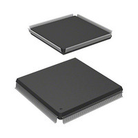
HD6417727F160V Renesas Electronics America, HD6417727F160V Datasheet - Page 107

HD6417727F160V
Manufacturer Part Number
HD6417727F160V
Description
MPU 3V 16K PB-FREE 240-QFP
Manufacturer
Renesas Electronics America
Series
SuperH® SH7700r
Datasheet
1.HD6417727BP100CV.pdf
(1098 pages)
Specifications of HD6417727F160V
Core Processor
SH-3 DSP
Core Size
32-Bit
Speed
160MHz
Connectivity
FIFO, SCI, SIO, SmartCard, USB
Peripherals
DMA, LCD, POR, WDT
Number Of I /o
104
Program Memory Type
ROMless
Ram Size
32K x 8
Voltage - Supply (vcc/vdd)
1.7 V ~ 2.05 V
Data Converters
A/D 6x10b; D/A 2x8b
Oscillator Type
Internal
Operating Temperature
-20°C ~ 75°C
Package / Case
240-QFP
Lead Free Status / RoHS Status
Lead free / RoHS Compliant
Eeprom Size
-
Program Memory Size
-
Available stocks
Company
Part Number
Manufacturer
Quantity
Price
Company:
Part Number:
HD6417727F160V
Manufacturer:
HITACHI
Quantity:
9
Company:
Part Number:
HD6417727F160V
Manufacturer:
Renesas Electronics America
Quantity:
10 000
Part Number:
HD6417727F160V
Manufacturer:
RENESAS/瑞萨
Quantity:
20 000
- Current page: 107 of 1098
- Download datasheet (7Mb)
2. Addition index register addressing:
3. Increment address register addressing:
There is an index register for each address pointer. The R8 register is the index register (Ix) for the
X memory address register (Ax), and the R9 register is the index register (Iy) for the Y memory
address register (Ay).
The X and Y data transfer instructions perform word-length processing, and use 16-bit access to
the X/Y data memory. A value of 2 is therefore added to the address register in the increment
processing. To perform decrementing, –2 is set in the index register and addition index register
addressing is specified. In X/Y data addressing, only bits 1 to 15 of the address pointer are valid.
When using X/Y data addressing, 0 must always be written to bit 0 of the address pointer and
index register.
X/Y data transfer addressing is shown in figure 2.12. When accessing X and Y memory using the
X and Y buses, the upper word of Ax (R4 or R5) and Ay (R6 or R7) is ignored. The result of
@AY+ or @Ay + Iy is stored in the lower word of Ay, while the upper word retains its original
value.
The Ax and Ay registers are address pointers. After a data transfer, the value of the Ix or Iy
register is added to each (post-increment).
The Ax and Ay registers are address pointers. After a data transfer, they are each incremented
by 2 (post- increment).
Note: Three address processing methods:
+2 (INC)
+0 (no update)
1. Increment
2. Index register addition (Ix/Iy)
3. No increment
Post-updating is used in all cases.
The address pointer can be decremented by setting −2/−4 in the index register.
R8[Ix]
Figure 2.12 X and Y Data Transfer Addressing
ALU
R4[Ax]
R5[Ax]
+2 (INC)
+0 (no update)
Rev.6.00 Mar. 27, 2009 Page 49 of 1036
R9[Iy]
AU: Adder provided
AU
for DSP addressing
REJ09B0254-0600
R6[Ay]
R7[Ay]
Section 2 CPU
Related parts for HD6417727F160V
Image
Part Number
Description
Manufacturer
Datasheet
Request
R

Part Number:
Description:
KIT STARTER FOR M16C/29
Manufacturer:
Renesas Electronics America
Datasheet:

Part Number:
Description:
KIT STARTER FOR R8C/2D
Manufacturer:
Renesas Electronics America
Datasheet:

Part Number:
Description:
R0K33062P STARTER KIT
Manufacturer:
Renesas Electronics America
Datasheet:

Part Number:
Description:
KIT STARTER FOR R8C/23 E8A
Manufacturer:
Renesas Electronics America
Datasheet:

Part Number:
Description:
KIT STARTER FOR R8C/25
Manufacturer:
Renesas Electronics America
Datasheet:

Part Number:
Description:
KIT STARTER H8S2456 SHARPE DSPLY
Manufacturer:
Renesas Electronics America
Datasheet:

Part Number:
Description:
KIT STARTER FOR R8C38C
Manufacturer:
Renesas Electronics America
Datasheet:

Part Number:
Description:
KIT STARTER FOR R8C35C
Manufacturer:
Renesas Electronics America
Datasheet:

Part Number:
Description:
KIT STARTER FOR R8CL3AC+LCD APPS
Manufacturer:
Renesas Electronics America
Datasheet:

Part Number:
Description:
KIT STARTER FOR RX610
Manufacturer:
Renesas Electronics America
Datasheet:

Part Number:
Description:
KIT STARTER FOR R32C/118
Manufacturer:
Renesas Electronics America
Datasheet:

Part Number:
Description:
KIT DEV RSK-R8C/26-29
Manufacturer:
Renesas Electronics America
Datasheet:

Part Number:
Description:
KIT STARTER FOR SH7124
Manufacturer:
Renesas Electronics America
Datasheet:

Part Number:
Description:
KIT STARTER FOR H8SX/1622
Manufacturer:
Renesas Electronics America
Datasheet:

Part Number:
Description:
KIT DEV FOR SH7203
Manufacturer:
Renesas Electronics America
Datasheet:


