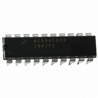
MC68HC908JB8JPE Freescale Semiconductor, MC68HC908JB8JPE Datasheet - Page 102

MC68HC908JB8JPE
Manufacturer Part Number
MC68HC908JB8JPE
Description
IC MCU FLASH 8BIT 8K 20-DIP
Manufacturer
Freescale Semiconductor
Series
HC08r
Datasheet
1.MC908JB8JDWE.pdf
(286 pages)
Specifications of MC68HC908JB8JPE
Core Processor
HC08
Core Size
8-Bit
Speed
3MHz
Connectivity
USB
Peripherals
LVD, POR, PWM
Number Of I /o
13
Program Memory Size
8KB (8K x 8)
Program Memory Type
FLASH
Ram Size
256 x 8
Voltage - Supply (vcc/vdd)
4 V ~ 5.5 V
Oscillator Type
Internal
Operating Temperature
0°C ~ 70°C
Package / Case
20-DIP (0.300", 7.62mm)
Controller Family/series
HC08
No. Of I/o's
13
Ram Memory Size
256Byte
Cpu Speed
3MHz
No. Of Timers
1
Embedded Interface Type
USB
Rohs Compliant
Yes
Processor Series
HC08JB
Core
HC08
Data Bus Width
8 bit
Data Ram Size
256 B
Interface Type
USB
Maximum Clock Frequency
3 MHz
Number Of Programmable I/os
37
Number Of Timers
2
Operating Supply Voltage
4 V to 5.5 V
Maximum Operating Temperature
+ 70 C
Mounting Style
Through Hole
Development Tools By Supplier
FSICEBASE, DEMO908GZ60E, M68EML08GZE, KITUSBSPIDGLEVME, KITUSBSPIEVME, KIT33810EKEVME
Minimum Operating Temperature
0 C
Lead Free Status / RoHS Status
Lead free / RoHS Compliant
Eeprom Size
-
Data Converters
-
Lead Free Status / Rohs Status
Details
- Current page: 102 of 286
- Download datasheet (2Mb)
System Integration Module (SIM)
8.4.2.5 Low-Voltage Inhibit (LVI) Reset
8.4.2.6 Universal Serial Bus Reset
8.4.2.7 Registers Values After Different Resets
Technical Data
102
NOTE:
The low-voltage inhibit module (LVI) asserts its output to the SIM when
the V
reset status register (RSR) is set, and the external reset pin (RST) is held
low while the SIM counter counts out 4096 OSCXCLK cycles. Sixty-four
OSCXCLK cycles later, the CPU is released from reset to allow the reset
vector sequence to occur. The SIM actively pulls down the RST pin for
all internal reset sources.
The USB module will detect a reset signaled on the bus by the presence
of an extended SE0 at the USB data pins of a device. The MCU seeing
a single-ended 0 on its USB data inputs for more than 2.5
signal as a reset. After the reset is removed, the device will be in the
attached, but not yet addressed or configured, state (refer to Section 9.1
USB Devices of the Universal Serial Bus Specification Rev. 1.1). The
device must be able to accept the device address via a SET_ADDRESS
command (refer to Section 9.4 of the Universal Serial Bus Specification
Rev. 1.1) no later than 10ms after the reset is removed.
USB reset can be disabled to generate an internal reset, instead, a USB
interrupt can be generated. (See
(CONFIG).)
USB reset is disabled when the USB module is disabled by clearing the
USBEN bit of the USB Address Register (UADDR).
Some registers are reset by POR or LVI reset only.
registers or register bits which are unaffected by normal resets.
DD
voltage falls to the LVI reset voltage, V
System Integration Module (SIM)
MC68HC908JB8•MC68HC08JB8•MC68HC08JT8 — Rev. 2.3
Section 5. Configuration Register
TRIP
Freescale Semiconductor
Table 8-3
. The LVI bit in the
µ
s treats that
shows the
Related parts for MC68HC908JB8JPE
Image
Part Number
Description
Manufacturer
Datasheet
Request
R
Part Number:
Description:
Manufacturer:
Freescale Semiconductor, Inc
Datasheet:
Part Number:
Description:
Manufacturer:
Freescale Semiconductor, Inc
Datasheet:
Part Number:
Description:
Manufacturer:
Freescale Semiconductor, Inc
Datasheet:
Part Number:
Description:
Manufacturer:
Freescale Semiconductor, Inc
Datasheet:
Part Number:
Description:
Manufacturer:
Freescale Semiconductor, Inc
Datasheet:
Part Number:
Description:
Manufacturer:
Freescale Semiconductor, Inc
Datasheet:
Part Number:
Description:
Manufacturer:
Freescale Semiconductor, Inc
Datasheet:
Part Number:
Description:
Manufacturer:
Freescale Semiconductor, Inc
Datasheet:
Part Number:
Description:
Manufacturer:
Freescale Semiconductor, Inc
Datasheet:
Part Number:
Description:
Manufacturer:
Freescale Semiconductor, Inc
Datasheet:
Part Number:
Description:
Manufacturer:
Freescale Semiconductor, Inc
Datasheet:
Part Number:
Description:
Manufacturer:
Freescale Semiconductor, Inc
Datasheet:
Part Number:
Description:
Manufacturer:
Freescale Semiconductor, Inc
Datasheet:
Part Number:
Description:
Manufacturer:
Freescale Semiconductor, Inc
Datasheet:
Part Number:
Description:
Manufacturer:
Freescale Semiconductor, Inc
Datasheet:


