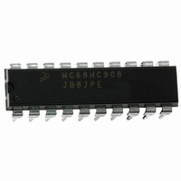
MC68HC908JB8JPE Freescale Semiconductor, MC68HC908JB8JPE Datasheet - Page 62

MC68HC908JB8JPE
Manufacturer Part Number
MC68HC908JB8JPE
Description
IC MCU FLASH 8BIT 8K 20-DIP
Manufacturer
Freescale Semiconductor
Series
HC08r
Datasheet
1.MC908JB8JDWE.pdf
(286 pages)
Specifications of MC68HC908JB8JPE
Core Processor
HC08
Core Size
8-Bit
Speed
3MHz
Connectivity
USB
Peripherals
LVD, POR, PWM
Number Of I /o
13
Program Memory Size
8KB (8K x 8)
Program Memory Type
FLASH
Ram Size
256 x 8
Voltage - Supply (vcc/vdd)
4 V ~ 5.5 V
Oscillator Type
Internal
Operating Temperature
0°C ~ 70°C
Package / Case
20-DIP (0.300", 7.62mm)
Controller Family/series
HC08
No. Of I/o's
13
Ram Memory Size
256Byte
Cpu Speed
3MHz
No. Of Timers
1
Embedded Interface Type
USB
Rohs Compliant
Yes
Processor Series
HC08JB
Core
HC08
Data Bus Width
8 bit
Data Ram Size
256 B
Interface Type
USB
Maximum Clock Frequency
3 MHz
Number Of Programmable I/os
37
Number Of Timers
2
Operating Supply Voltage
4 V to 5.5 V
Maximum Operating Temperature
+ 70 C
Mounting Style
Through Hole
Development Tools By Supplier
FSICEBASE, DEMO908GZ60E, M68EML08GZE, KITUSBSPIDGLEVME, KITUSBSPIEVME, KIT33810EKEVME
Minimum Operating Temperature
0 C
Lead Free Status / RoHS Status
Lead free / RoHS Compliant
Eeprom Size
-
Data Converters
-
Lead Free Status / Rohs Status
Details
- Current page: 62 of 286
- Download datasheet (2Mb)
FLASH Memory
4.9.1 Variables
4.9.2 ERASE Routine
Technical Data
62
The ROM-resident routines use three variables: CTRLBYT, CPUSPD
and LADDR; and one data buffer. The minimum size of the data buffer
is one byte and the maximum size is 64 bytes.
CPUSPD must be set before calling the ERASE or PROGRAM routine,
and should be set to four times the value of the CPU internal bus speed
in MHz. For example: for CPU speed of 3MHz, CPUSPD should be set
to 12.
The ERASE routine erases the entire FLASH memory. The routine does
not check for a blank range before or after erase.
CTRLBYT
Routine
Calling Address
Stack Use
Input
DATABUF
CPUSPD
Variable
LADDR
Table 4-2. ROM-Resident Routine Variables
FLASH Memory
$004C–$008B
$004A–$004B
MC68HC908JB8•MC68HC08JB8•MC68HC08JT8 — Rev. 2.3
Address
ERASE
$FC06
5 Bytes
CPUSPD — CPU speed
HX —
CTRLBYT — Mass erase
$0048
$0049
Table 4-3. ERASE Routine
Mass erase if bit 6 = 1
Contains any address in the range to be
erased
Control byte for setting mass erase.
Timing adjustment for different CPU
speeds.
Last FLASH address to be programmed.
Data buffer for programming and verifying.
Description
Freescale Semiconductor
Related parts for MC68HC908JB8JPE
Image
Part Number
Description
Manufacturer
Datasheet
Request
R
Part Number:
Description:
Manufacturer:
Freescale Semiconductor, Inc
Datasheet:
Part Number:
Description:
Manufacturer:
Freescale Semiconductor, Inc
Datasheet:
Part Number:
Description:
Manufacturer:
Freescale Semiconductor, Inc
Datasheet:
Part Number:
Description:
Manufacturer:
Freescale Semiconductor, Inc
Datasheet:
Part Number:
Description:
Manufacturer:
Freescale Semiconductor, Inc
Datasheet:
Part Number:
Description:
Manufacturer:
Freescale Semiconductor, Inc
Datasheet:
Part Number:
Description:
Manufacturer:
Freescale Semiconductor, Inc
Datasheet:
Part Number:
Description:
Manufacturer:
Freescale Semiconductor, Inc
Datasheet:
Part Number:
Description:
Manufacturer:
Freescale Semiconductor, Inc
Datasheet:
Part Number:
Description:
Manufacturer:
Freescale Semiconductor, Inc
Datasheet:
Part Number:
Description:
Manufacturer:
Freescale Semiconductor, Inc
Datasheet:
Part Number:
Description:
Manufacturer:
Freescale Semiconductor, Inc
Datasheet:
Part Number:
Description:
Manufacturer:
Freescale Semiconductor, Inc
Datasheet:
Part Number:
Description:
Manufacturer:
Freescale Semiconductor, Inc
Datasheet:
Part Number:
Description:
Manufacturer:
Freescale Semiconductor, Inc
Datasheet:


