MC68HC908JB8JPE Freescale Semiconductor, MC68HC908JB8JPE Datasheet - Page 212
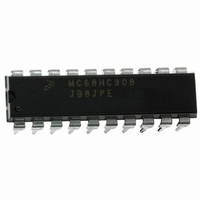
MC68HC908JB8JPE
Manufacturer Part Number
MC68HC908JB8JPE
Description
IC MCU FLASH 8BIT 8K 20-DIP
Manufacturer
Freescale Semiconductor
Series
HC08r
Datasheet
1.MC908JB8JDWE.pdf
(286 pages)
Specifications of MC68HC908JB8JPE
Core Processor
HC08
Core Size
8-Bit
Speed
3MHz
Connectivity
USB
Peripherals
LVD, POR, PWM
Number Of I /o
13
Program Memory Size
8KB (8K x 8)
Program Memory Type
FLASH
Ram Size
256 x 8
Voltage - Supply (vcc/vdd)
4 V ~ 5.5 V
Oscillator Type
Internal
Operating Temperature
0°C ~ 70°C
Package / Case
20-DIP (0.300", 7.62mm)
Controller Family/series
HC08
No. Of I/o's
13
Ram Memory Size
256Byte
Cpu Speed
3MHz
No. Of Timers
1
Embedded Interface Type
USB
Rohs Compliant
Yes
Processor Series
HC08JB
Core
HC08
Data Bus Width
8 bit
Data Ram Size
256 B
Interface Type
USB
Maximum Clock Frequency
3 MHz
Number Of Programmable I/os
37
Number Of Timers
2
Operating Supply Voltage
4 V to 5.5 V
Maximum Operating Temperature
+ 70 C
Mounting Style
Through Hole
Development Tools By Supplier
FSICEBASE, DEMO908GZ60E, M68EML08GZE, KITUSBSPIDGLEVME, KITUSBSPIEVME, KIT33810EKEVME
Minimum Operating Temperature
0 C
Lead Free Status / RoHS Status
Lead free / RoHS Compliant
Eeprom Size
-
Data Converters
-
Lead Free Status / Rohs Status
Details


Input/Output Ports (I/O)
12.7 Port E
Technical Data
212
When bit DDRDx is a logic 1, reading address $0003 reads the PTDx
data latch. When bit DDRDx is a logic 0, reading address $0003 reads
the voltage level on the pin. The data latch can always be written,
regardless of the state of its data direction bit.
the operation of the port D pins.
Port E is a 5-bit special function port that shares three of its pins with the
timer interface module (TIM) and two of its pins with the USB data pins
D+ and D–. PTE4 and PTE3 are open drain when configured as output.
NOTES:
1. X = don’t care.
2. Hi-Z = high impedance.
3. Writing affects data register, but does not affect input.
DDRD
Bit
0
1
READ DDRD ($0007)
WRITE DDRD ($0007)
WRITE PTD ($0003)
READ PTD ($0003)
PTD Bit
Input/Output Ports (I/O)
X
X
(1)
Table 12-5. Port D Pin Functions
Figure 12-13. Port D I/O Circuit
MC68HC908JB8•MC68HC08JB8•MC68HC08JT8 — Rev. 2.3
RESET
I/O Pin Mode
Input, Hi-Z
Output
(2)
DDRDx
PTDx
Read/Write
DDRD[7:0]
DDRD[7:0]
Accesses
to DDRD
Table 12-5
PTD[7:0]
Freescale Semiconductor
Read
Accesses to PTD
Pin
summarizes
PTD[7:0]
PTD[7:0]
Write
PTDx
(3)
Related parts for MC68HC908JB8JPE
Image
Part Number
Description
Manufacturer
Datasheet
Request
R

Part Number:
Description:
Manufacturer:
Freescale Semiconductor, Inc
Datasheet:
Part Number:
Description:
Manufacturer:
Freescale Semiconductor, Inc
Datasheet:
Part Number:
Description:
Manufacturer:
Freescale Semiconductor, Inc
Datasheet:
Part Number:
Description:
Manufacturer:
Freescale Semiconductor, Inc
Datasheet:
Part Number:
Description:
Manufacturer:
Freescale Semiconductor, Inc
Datasheet:
Part Number:
Description:
Manufacturer:
Freescale Semiconductor, Inc
Datasheet:
Part Number:
Description:
Manufacturer:
Freescale Semiconductor, Inc
Datasheet:
Part Number:
Description:
Manufacturer:
Freescale Semiconductor, Inc
Datasheet:
Part Number:
Description:
Manufacturer:
Freescale Semiconductor, Inc
Datasheet:
Part Number:
Description:
Manufacturer:
Freescale Semiconductor, Inc
Datasheet:
Part Number:
Description:
Manufacturer:
Freescale Semiconductor, Inc
Datasheet:
Part Number:
Description:
Manufacturer:
Freescale Semiconductor, Inc
Datasheet:
Part Number:
Description:
Manufacturer:
Freescale Semiconductor, Inc
Datasheet:
Part Number:
Description:
Manufacturer:
Freescale Semiconductor, Inc
Datasheet:
Part Number:
Description:
Manufacturer:
Freescale Semiconductor, Inc
Datasheet: