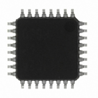
M37544G2AGP#U0 Renesas Electronics America, M37544G2AGP#U0 Datasheet - Page 26

M37544G2AGP#U0
Manufacturer Part Number
M37544G2AGP#U0
Description
IC 740 MCU OTP 8K 32LQFP
Manufacturer
Renesas Electronics America
Series
740/38000r
Specifications of M37544G2AGP#U0
Core Processor
740
Core Size
8-Bit
Speed
8MHz
Connectivity
SIO, UART/USART
Peripherals
WDT
Number Of I /o
25
Program Memory Size
8KB (8K x 8)
Program Memory Type
QzROM
Ram Size
256 x 8
Voltage - Supply (vcc/vdd)
4 V ~ 5.5 V
Data Converters
A/D 6x8b
Oscillator Type
Internal
Operating Temperature
-20°C ~ 85°C
Package / Case
32-LQFP
Lead Free Status / RoHS Status
Lead free / RoHS Compliant
Eeprom Size
-
Available stocks
Company
Part Number
Manufacturer
Quantity
Price
REJ03B0108-0103
page 24 of 72
7544 Group (QzROM version)
Fig. 20 Interrupt sequence
Fig. 21 Timing of interrupt request generation, interrupt request bit, and interrupt acceptance
When setting the followings, the interrupt request bit of the corre-
sponding interrupt may be set to “1”.
<When switching external interrupt active edge>
• INT
• INT
• CNTR
• CNTR
(bit 0 of Interrupt edge selection register (address 003A
(bit 1 of Interrupt edge selection register)
(bit 2 of timer X mode register (address 002B
(bit 6 of timer A mode register (address 100D
Notes on Interrupts
0
1
interrupt edge selection bit
interrupt edge selection bit
0
1
Internal clock φ
active edge switch bit
active edge switch bit
SYNC
Rev.1.03
(1) The interrupt request bit for an interrupt request generated during period 1 is set to “1” at timing point IR1.
(2) The interrupt request bit for an interrupt request generated during period 2 is set to “1” at timing point IR1 or IR2.
The timing point at which the bit is set to “1” varies depending on conditions. When two or more interrupt
requests are generated during the period 2, each request bit may be set to “1” at timing point IR1 or IR2
separately.
T1 T2 T3 : Interrupt acceptance timing points
IR1 IR2 : Timings points at which the interrupt request bit is set to “1”.
Note : Period 2 indicates the last φ cycle during one instruction cycle.
T1
Address bus
SYNC : CPU operation code fetch cycle
B
A
SPS
Data bus
L
L
Mar 31, 2009
, B
, A
SYNC
H
H
WR
Instruction cycle
RD
φ
: Vector address of each interrupt
: Jump destination address of each interrupt
: “00
(This is an internal signal that cannot be observed from the external unit.)
([SPS] is a page selected by the stack page selection bit of CPU mode register.)
16
” or “01
16
16
PC
Not used
))
))
16
”
IR1 T2
S,SPS
16
))
PC
Push onto stack
S-1,SPS S-2,SPS
Vector fetch
H
PC
L
If it is not necessary to generate an interrupt synchronized with
these settings, take the following sequence.
(1) Set the corresponding enable bit to “0” (disabled).
(2) Set the interrupt edge selection bit (the active edge switch bit)
(3) Set the corresponding interrupt request bit to “0” after one or
(4) Set the corresponding interrupt enable bit to “1” (enabled).
PS
Push onto stack
Vector fetch
or the interrupt source bit.
more instructions have been executed.
B
L
A
L
B
H
A
H
Execute interrupt
routine
A
L
,A
H
IR2 T3
Instruction cycle


